A p-type nitride epitaxial structure, preparation method and semiconductor device
An epitaxial structure and nitride technology, which is applied in semiconductor/solid-state device manufacturing, electrical components, final product manufacturing, etc., can solve the problem of carrier concentration decline, inability to suppress the self-compensation effect of doping elements, and low activation rate of doping elements and other problems, to achieve the effect of suppressing self-compensation effect, promoting good surface morphology and increasing solubility
- Summary
- Abstract
- Description
- Claims
- Application Information
AI Technical Summary
Problems solved by technology
Method used
Image

Examples
preparation example Construction
[0052] The above-mentioned P-type nitride epitaxial structure can be prepared by the following preparation method, including the following steps:
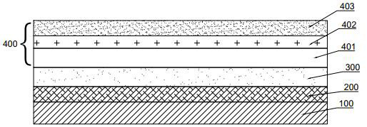
[0053] S1, growing the U-type nitride layer 200 on the substrate 100;
[0054] Specifically, a U-type nitride layer 200 of 1 μm-3 μm is grown on the substrate; the U-type nitride layer 200 makes the foreign substrate transition to a flat GaN material layer;
[0055] S2, growing a P-type nitride pre-layer 300 on the U-type nitride layer 200, wherein the P-type nitride pre-layer 300 is lightly doped with Mg;
[0056] Specifically, a P-type nitride pre-layer 300 with a thickness of 0.5um-1.5 μm is grown on the U-type nitride layer 200; wherein, the doping concentration of Mg element in the P-type nitride pre-layer 300 is 1E18cm -3 -1E19cm -3 ;
[0057] The lightly doped P-type nitride pre-layer 300 avoids the influence of the weak N-type of the U-type nitride layer on the subsequent P-type layer, and eliminates the influence of the...
Embodiment 1
[0070] This embodiment prepares and tests the P-type GaN epitaxial structure, which specifically includes the following steps:
[0071] 1) A 2um U-type GaN layer is grown on a sapphire substrate;
[0072] 2) Grow a 1um P-type GaN pre-layer on the U-type GaN layer, where the doping concentration of Mg is about 1E19cm -3 ;
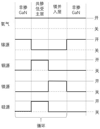
[0073] 3) Set the growth temperature to 1050°C, pass in the gallium source, and grow the undoped GaN layer for 15s;
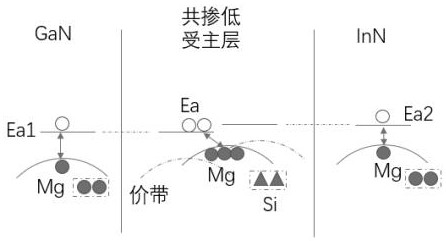
[0074] 4) Turn off the gallium source, pass in the indium source and the silicon source, cool down to 950 ℃ to grow the co-doped low acceptor layer, the growth time is 5s, where, In / Ga (molar ratio)=2, the doping concentration of Si is 5E17cm -3 ;
[0075] 5) Turn off the indium source and the silicon source, only pass in the magnesium source, and grow the Mg doping incorporated layer for 5s, where the doping concentration of Mg is 5E20cm -3 ;
[0076] 6) According to steps 3), 4) and 5), the P-type GaN composite layer is formed by cycli...
Embodiment 2
[0094] In order to further illustrate the function of the P-type GaN pre-layer in the present invention, the thickness of the P-type GaN pre-layer is changed in this embodiment compared with Embodiment 1, and the rest is the same as that of Embodiment 1;
[0095] Result: Under the test condition of the Hall current of 1uA, the Hall effect test is carried out:
[0096] 1) When the thickness of the P-type GaN pre-layer is 0.5um, the doping concentration of Mg is about 1E18cm -3 , the carrier concentration of the prepared P-type GaN layer is 5.4E18cm -3 ;
[0097] 2) When the thickness of the P-type GaN pre-layer is 1.5um, the doping concentration of Mg is about 1E19cm -3 , the carrier concentration of the prepared P-type GaN layer is 6.2E18cm -3 ;
[0098] The results show that compared with the non-P-type GaN pre-layer in Comparative Example 1, the two thickness pre-layers of Example 2 have higher carrier concentrations, which further proves that the P-type GaN pre-layer ha...
PUM
| Property | Measurement | Unit |
|---|---|---|
| thickness | aaaaa | aaaaa |
| thickness | aaaaa | aaaaa |
| thickness | aaaaa | aaaaa |
Abstract
Description
Claims
Application Information
 - R&D
- Intellectual Property
- Life Sciences
- Materials
- Tech Scout
- Unparalleled Data Quality
- Higher Quality Content
- 60% Fewer Hallucinations
Browse by: Latest US Patents, China's latest patents, Technical Efficacy Thesaurus, Application Domain, Technology Topic, Popular Technical Reports.
© 2025 PatSnap. All rights reserved.Legal|Privacy policy|Modern Slavery Act Transparency Statement|Sitemap|About US| Contact US: help@patsnap.com