Metal-oxide-semiconductor field-effect transistor and manufacturing method thereof

A technology of oxide semiconductor and field effect transistor, which is applied in the field of metal oxide semiconductor field effect transistor and its production, can solve the problem of device reliability, increase of device gate resistance, difficult filling of gate metal, etc., to reduce resistance , change the cross-sectional area, the effect of flexible resistance

Active Publication Date: 2021-10-29
河南启昂半导体有限公司 +1
View PDF6 Cites 0 Cited by
  • Summary
  • Abstract
  • Description
  • Claims
  • Application Information

AI Technical Summary

Problems solved by technology

Due to the continuous shrinking of the size of semiconductor devices, the process window of gap fill (gap filling) is also getting smaller and smaller. When it develops below 28nm, the process of gap fill is very difficult, which makes it difficult to fill the gate metal.
When the filling capacity is insufficient, it is very likely to cause voids in the metal gate. On the one hand, this may lead to an increase in the gate resistance of the device, and on the other hand, it may also cause some reliability problems in the device.

Method used


Image

  • Metal-oxide-semiconductor field-effect transistor and manufacturing method thereof
  • Metal-oxide-semiconductor field-effect transistor and manufacturing method thereof
  • Metal-oxide-semiconductor field-effect transistor and manufacturing method thereof

Examples


Embodiment Construction

[0032] The following will clearly and completely describe the technical solutions in the embodiments of the present invention. Obviously, the described embodiments are only some of the embodiments of the present invention, rather than all the embodiments. Based on the embodiments of the present invention, all other embodiments obtained by persons of ordinary skill in the art without making creative efforts belong to the protection scope of the present invention.

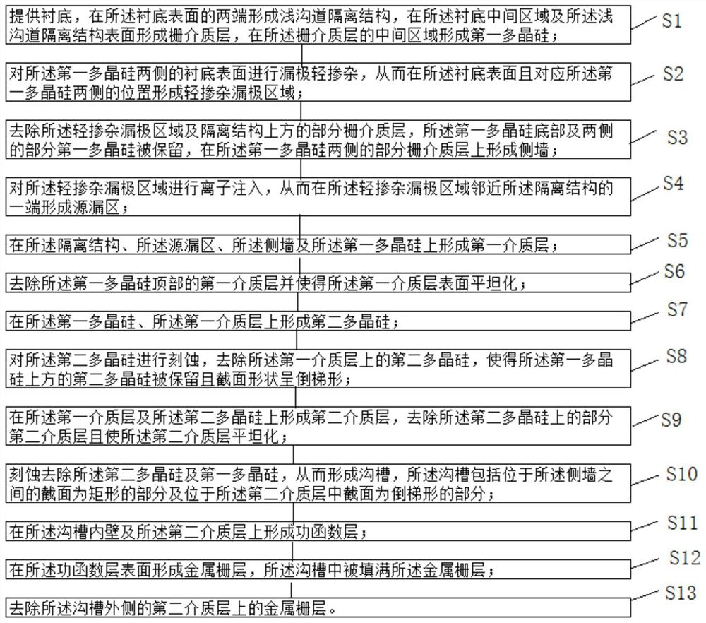
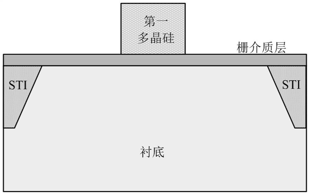
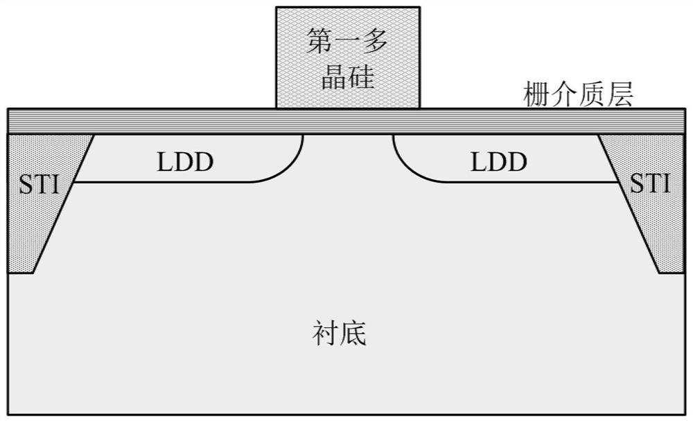
[0033] see Figure 1-Figure 15 , figure 1 It is a flow chart of the fabrication method of the metal oxide semiconductor field effect transistor of the present invention, Figure 2-Figure 15 for figure 1 A schematic structural view of each step in the fabrication method of the metal oxide semiconductor field effect transistor shown. The manufacturing method of the metal oxide semiconductor field effect transistor includes the following steps.

[0034] Step S1, see figure 2 , providing a substrate, forming a shal...


PUM

PropertyMeasurementUnit
angleaaaaaaaaaa
thicknessaaaaaaaaaa

Abstract

The invention relates to a metal oxide semiconductor field effect transistor and a manufacturing method thereof. The metal oxide semiconductor field effect transistor obtained by the manufacturing method includes a substrate, a shallow trench isolation structure formed at both ends of the substrate surface, a gate dielectric layer formed on the surface of the middle region of the substrate, and a gate dielectric layer formed at both ends of the gate dielectric layer. The formed sidewall, the lightly doped drain region formed on the substrate under the gate dielectric layer under the sidewall, and the source and drain formed on the substrate surface between the lightly doped drain region and the shallow trench isolation structure region, the first dielectric layer formed on the source and drain regions and the shallow trench isolation structure, the second dielectric layer formed on the first dielectric layer, the trench surrounded by the second dielectric layer and sidewalls, and the trench formed in the trench The work function layer of the side wall, the metal gate layer forming the surface of the work function layer and filling in the groove, wherein the groove includes a part with a rectangular cross section between the side walls and an inverted trapezoidal cross section in the second dielectric layer part.

Description

【Technical field】 [0001] The invention relates to the technical field of semiconductor manufacturing technology, in particular to a metal oxide semiconductor field effect transistor and a manufacturing method thereof. 【Background technique】 [0002] The main device in an integrated circuit, especially a VLSI, is a metal oxide semiconductor field effect transistor (MOS transistor for short). Since the MOS tube was invented, its geometric size has been continuously reduced. In this context, various practical and fundamental limitations and technical challenges begin to emerge, and further scaling down of device dimensions is becoming more and more difficult. As the composite metal oxide semiconductor structure (CMOS) manufacturing process shrinks to below 32nm level, the High K Metal Gate technology, referred to as HKMG, is introduced. [0003] Among them, in the preparation of MOS transistor devices and circuits, the most challenging thing is the high gate leakage current c...

Claims


Application Information

Patent Timeline
Patent Type & Authority Patents(China)
IPC IPC(8): H01L29/78H01L21/336H01L29/423
CPCH01L29/4236H01L29/66545H01L29/78
Inventor 不公告发明人
Owner 河南启昂半导体有限公司
Why Eureka
Try Eureka