Preparation method of GaN-based LED chip with performance optimization effect

A LED chip and performance technology, applied in the direction of electrical components, circuits, semiconductor devices, etc., can solve the problems of easy formation of open circuit, metal interconnection fracture, short circuit, etc., to reduce leakage current, improve reliability, and optimize transportation characteristics Effect

Active Publication Date: 2018-03-06
JIANGSU XGL OPTOELECTRONICS
View PDF10 Cites 5 Cited by
  • Summary
  • Abstract
  • Description
  • Claims
  • Application Information

AI Technical Summary

Problems solved by technology

For multiple light-emitting units of high-voltage LED chips, when laying electrode bridges in deep trenches, if SiO 2 The insulation layer is not well protected or the metal interconnection is broken, which is prone to problems such as open circuit, leakage and open circuit after conduction
[0004] Currently, if Figure 12 and Figure 13 As shown, the side wall of the isolation trench 12 of the existing LED chip is etched relatively steeply (the angle between the side wall and the substrate 1 is about 70° o ), SiO 2 In the uneven deposition of the side wall, there will be relatively thin or even undeposited places, which is easy to form a short circuit; at the same time, it is not conducive to the uniform deposition of the metal electrode film on the side wall, and the side wall metal film is relatively thin, which is easy to form an open circuit; at the same time Also because the side wall is steep, after depositing the metal electrode, it is obvious that the thickness of the metal is poorly distributed on the side wall, and there is even a layering phenomenon at the bottom, so that due to the different thickness of the metal, the resistance value of the resistance will also be unevenly distributed. uniform

Method used


Image

  • Preparation method of GaN-based LED chip with performance optimization effect
  • Preparation method of GaN-based LED chip with performance optimization effect
  • Preparation method of GaN-based LED chip with performance optimization effect

Examples


Embodiment 1

[0038] Embodiment 1 Taking a high-voltage LED chip as an example, a preparation method for optimizing the performance of a GaN-based LED chip is characterized in that it includes the following steps:

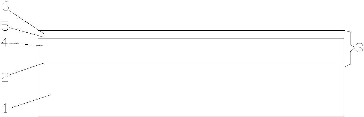
[0039] Such as figure 1 As shown, step 1. Fabricate the epitaxial layer: provide a substrate 1, grow buffer layer 2, N-GaN layer 4, multiple quantum wells 5, P-GaN layer 6 sequentially on the substrate 1, and complete GaN-based epitaxy The production of layer 3;

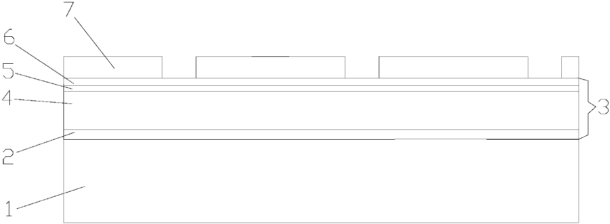
[0040] Such as figure 2 As shown, step 2. Fabricate the transparent conductive layer 7: use electron beam evaporation or magnetron sputtering technology to evaporate ITO on the upper surface of the GaN epitaxial layer 3, and use HCl solution to process the ITO through the shielding of the patterned photoresist. Etching to form a transparent conductive layer 7;

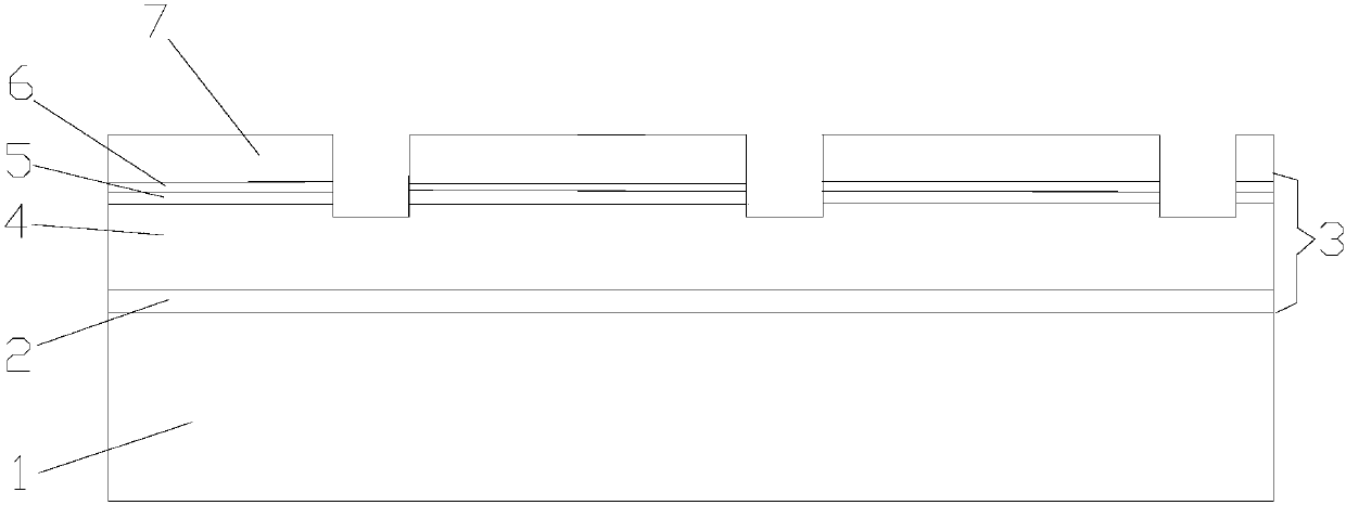
[0041] Such as image 3 As shown, step 3. Forming the N-electrode lead-out hole: under the cover of the patterned photoresist, continue to dry-etch the P...

Embodiment 2

[0049] Embodiment 2 Taking a flip-chip LED chip as an example, a preparation method for optimizing the performance of a GaN-based LED chip is characterized in that it includes the following steps:

[0050] Such as figure 1 As shown, step 1. Fabricate the epitaxial layer: provide a substrate 1, grow buffer layer 2, N-GaN layer 4, multiple quantum wells 5, P-GaN layer 6 sequentially on the substrate 1, and complete GaN-based epitaxy The production of layer 3;

[0051] Such as Figure 7 As shown, step 2. Fabricate the transparent conductive layer 7: use electron beam evaporation or magnetron sputtering technology to evaporate ITO on the upper surface of the GaN epitaxial layer 3, and use HCl solution to process the ITO through the shielding of the patterned photoresist. Etching to form a transparent conductive layer 7;

[0052] Such as Figure 8 As shown, step 3. Forming the N-electrode lead-out hole: under the cover of the patterned photoresist, continue to dry-etch the P-G...


PUM


Abstract

The invention provides a preparation method of a GaN-based LED chip with a performance optimization effect. The preparation method comprises the following steps of manufacturing an epitaxial layer, manufacturing a transparent conductive layer, manufacturing an N electrode leading-out hole, removing photoresist, forming an isolation trench, removing the photoresist and an SiO<2> mask layer, manufacturing an insulating layer and manufacturing an electrode. By adoption of an SiO<2> mask layer over etching method and by combination of inductively coupled plasma (ICP) etching, the side wall of theLED chip isolation trench is of an inverted trapezoidal structure; for a flip-chip LED chip and a high-voltage LED chip, SiO<2> on the side wall of the isolation trench can be uniform in deposition, so that generation of an electric leakage condition can be prevented effectively, and production yield can be optimized; and for the high-voltage LED chip, when an electrode connecting bridge is paved,the electrode can reach the bottom of the isolation trench along the trapezoidal structure of the side wall, and then climbs to an electrode of another chip from the bottom of the isolation trench along the trapezoidal structure of the side wall, so that a fault phenomenon caused in side wall electrode bridging can be avoided, electrode stability is improved, LED damage probability is lowered andthe production yield is optimized.

Description

technical field [0001] The invention relates to a preparation method of a GaN-based LED chip, in particular to a preparation method for optimizing the performance of a GaN-based LED chip, and belongs to the technical field of LED chips. Background technique [0002] In GaN-based LED chips, the control of etched sidewall morphology is very important. Due to the very good chemical stability of GaN, the current etching of GaN is usually based on dry etching, including dry etching techniques such as electron cyclotron resonance plasma (ECR), inductively coupled plasma (ICP) and ion beam bombardment. [0003] The rapid development of high-voltage LED chips and flip-chip LED chips in recent years requires the formation of moderate-angle steps, which can not only effectively isolate but also adapt to the coverage of metal electrode interconnections between units. For flip-chip LED chips, deep grooves need to be etched, and finally SiO 2 The insulating layer protects the sidewalls...

Claims


Application Information

Patent Timeline
Patent Type & Authority Applications(China)
IPC IPC(8): H01L33/00
CPCH01L33/0075
Inventor 闫晓密黄慧诗王书宇张秀敏贾美琳
Owner JIANGSU XGL OPTOELECTRONICS
Why Eureka
Try Eureka