Radio frequency microsystem packaging module and manufacturing method thereof
A technology for encapsulating modules and manufacturing methods, which is applied in semiconductor/solid-state device manufacturing, electrical components, electric solid-state devices, etc., which can solve the problems of high cost, complex processing, and increased cost of RF front-end modules, so as to reduce the packaging size and eliminate coupling Function, the effect of improving electrical performance
- Summary
- Abstract
- Description
- Claims
- Application Information
AI Technical Summary
Problems solved by technology
Method used
Image
Examples
Embodiment 1
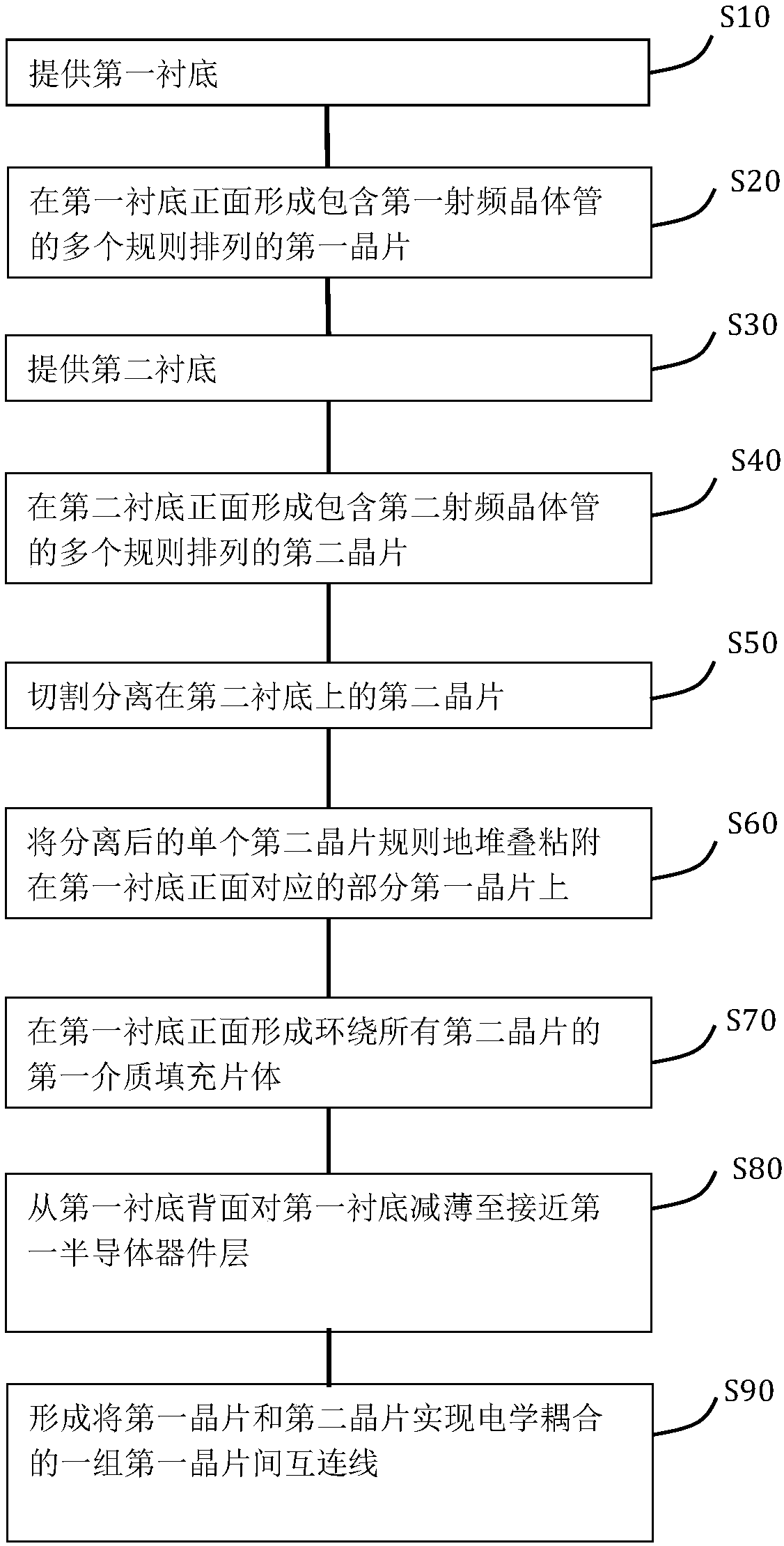
[0035] In Embodiment 1, the radio frequency microsystem packaging module and its manufacturing method in the first embodiment are described in combination with the manufacturing method of the radio frequency microsystem packaging module and the radio frequency microsystem packaging module formed by the method. refer to figure 1 , the radio frequency microsystem encapsulation module of the present embodiment comprises the steps:
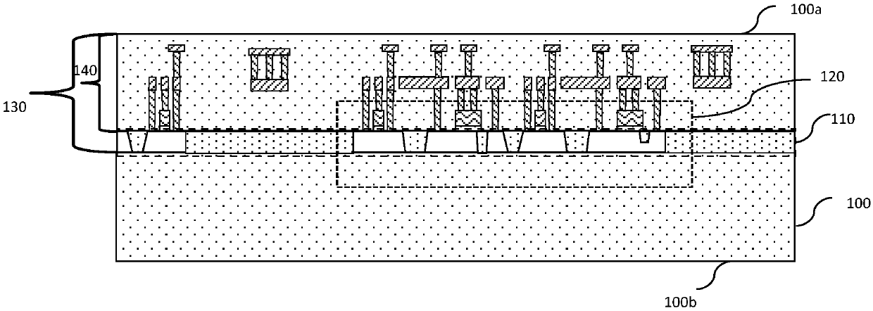
[0036] S10, providing a first substrate, the first substrate including the first semiconductor device layer on its front side;
[0037] S20, forming a plurality of regularly arranged first wafers including first radio frequency transistors on the first semiconductor device layer on the front side of the first substrate;
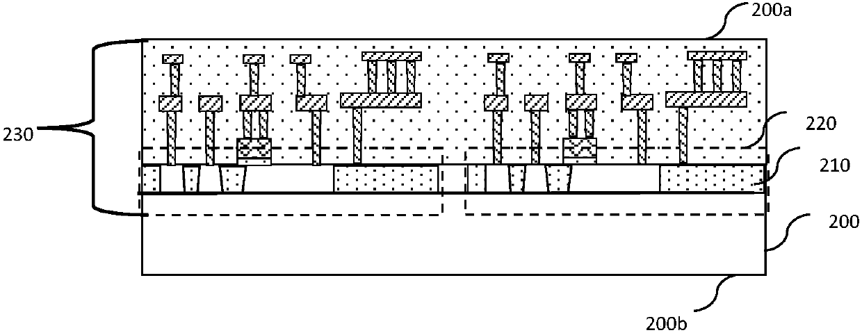
[0038] S30, providing a second substrate, the second substrate including a second semiconductor device layer on its front side;
[0039] S40, forming a plurality of regularly arranged second wafers including second radio frequency ...
Embodiment 2
[0078] In Embodiment 2, the radio frequency microsystem packaging module and its manufacturing method in the second embodiment are described in conjunction with the manufacturing method of the radio frequency microsystem packaging module and the radio frequency microsystem packaging module formed by the method. refer to figure 1 with Figure 8 , the radio frequency microsystem encapsulation module of the present embodiment comprises the steps:
[0079] S10, providing a first substrate, where the first substrate includes the first semiconductor device layer on the front side thereof.
[0080] S20, forming a plurality of regularly arranged first wafers including first radio frequency transistors on the first semiconductor device layer on the front side of the first substrate;
[0081] S30, providing a second substrate, the second substrate including a second semiconductor device layer on its front side;
[0082] S40, forming a plurality of regularly arranged second wafers inc...
Embodiment 3
[0111] In this embodiment, the same steps as in Embodiment 2 will not be repeated, the difference is that:
[0112] In this embodiment, the back of the third wafer is opposite to the front of the first wafer, and there are metal leads in the first dielectric filling sheet, and the metal leads are conductively interconnected with the first radio frequency transistor and the first radio frequency transistor in the first wafer. Describe the third chip.
[0113] Concrete steps are different from embodiment 2 in that:
[0114] refer to Figure 11 Before forming the first dielectric filling sheet in step S70, the interconnected metal leads 700 are formed on the front surface 100a of the first wafer and the front surface 500a of the third wafer, which can be formed by wire bonding well known to those skilled in the art. The metal lead 700 electrically interconnects the first RF transistor 120 on the first die and the third RF transistor 520 on the third die.
[0115] After that, t...
PUM
 Abstract
Description
Claims
Application Information
 - R&D
- Intellectual Property
- Life Sciences
- Materials
- Tech Scout
- Unparalleled Data Quality
- Higher Quality Content
- 60% Fewer Hallucinations
Browse by: Latest US Patents, China's latest patents, Technical Efficacy Thesaurus, Application Domain, Technology Topic, Popular Technical Reports.
© 2025 PatSnap. All rights reserved.Legal|Privacy policy|Modern Slavery Act Transparency Statement|Sitemap|About US| Contact US: help@patsnap.com


