
Chip packaging structure and manufacture procedure

A chip packaging structure, chip packaging technology, applied in semiconductor/solid-state device manufacturing, electrical components, electric solid devices, etc., can solve the problems of short package size, chip pollution overall structure, alignment offset, etc., to reduce the size of the package Effect

Inactive Publication Date: 2015-04-29
林登炎
View PDF8 Cites 0 Cited by
  • Summary
  • Abstract
  • Description
  • Claims
  • Application Information

AI Technical Summary

Problems solved by technology

[0004] However, for the application fields of mobile phones, mobile or handheld electronic devices that require lighter, thinner, shorter and smaller appearance, and more complex and powerful functions, the carrier board area of ​​the BGA package is quite large, and the solder balls need a certain amount of space. The size of the overall package cannot be further reduced, which drives the industry to develop a chip-scale package (Chip Scale Package, CSP) with a smaller package size. Usually, the package size is only 20% larger than the original chip.
[0005] However, the disadvantage of the above prior art is that no matter it is DIP package, QFP package, BGA package, or CSP package, the chip is placed in the mold first, and then the packaging material is injected to surround the chip, and the package is formed by heating and curing. As a result, the vertical height (thickness) and lateral size (area) of the final product cannot be reduced due to the limitations of mold forming, such as the fluidity of the packaging material and the mechanical strength of the package.
[0006] In addition, for chips with light-transmitting functions, such as optical imaging chips, additional processes are required to add one glass element at a time, and during the installation process, it is easy to cause contamination of the chip or alignment shift of the overall structure, etc. The problem

Method used


Image

  • Chip packaging structure and manufacture procedure
  • Chip packaging structure and manufacture procedure
  • Chip packaging structure and manufacture procedure

Examples


Embodiment Construction

[0041] The implementation of the present invention will be described in more detail below with reference to the figures and symbol numbers, so that those skilled in the art can implement it after studying this specification.

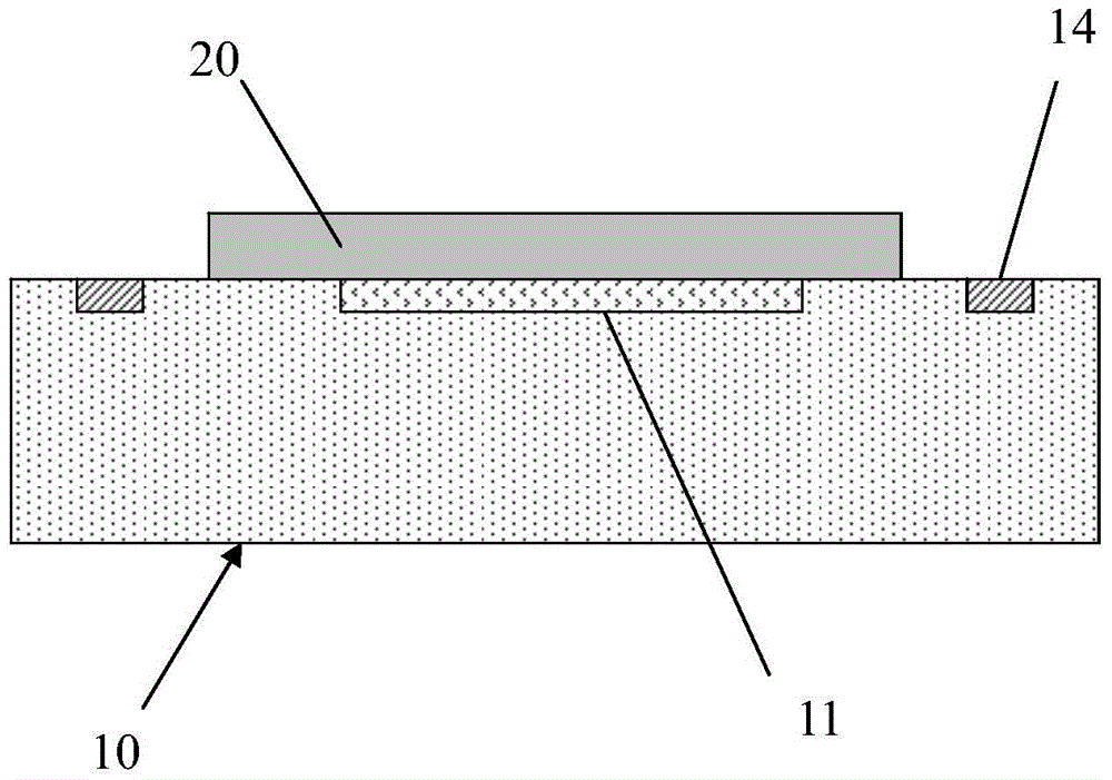
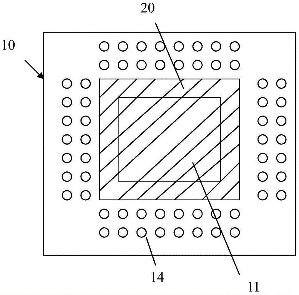
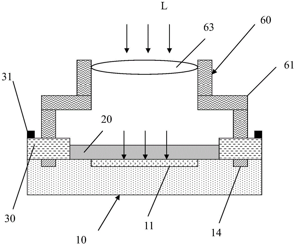
[0042] refer to figure 1 , is a schematic diagram of the chip packaging structure of the present invention. like figure 1 As shown, the chip packaging structure of the present invention mainly includes a chip 10 and a nano-deposition layer 20, wherein the chip 10 is, for example, an optical sensing chip, and has an electrical circuit (not shown in the figure), a photosensitive area 11, and a plurality of electrical connection pads 14, and the photosensitive region 11 and a plurality of electrical connection pads 14 are arranged on the upper surface of the chip 10, and the nano-deposited layer 20 covers the surface of the photosensitive region 11 in a semiconductor manufacturing process, that is, the nano-deposited layer 20 The lateral dimension is grea...


PUM

PropertyMeasurementUnit
Thicknessaaaaaaaaaa

Abstract

The invention discloses a chip packaging structure and a manufacture procedure. The structure comprises a chip and a nano deposition layer, wherein the chip is provided with an electrical circuit, a light sensation zone and a plurality of electrical connection gaskets, wherein the light sensation zone and the electrical connection gaskets are configured on the upper surface of the chip; the nano deposition layer covers the surface of the light sensation zone and exposes the electrical connection gaskets; the light sensation zone has a light sensation function, and the electrical connection gaskets are connected with the electrical circuit and used for connecting an external circuit or an electrical element; the nano deposition layer has electric insulativity and light transmission and has electrical insulation and isolation protection functions. The manufacture procedure comprises chip cleaning, formation of the nano deposition layer, cutting and carving of a wafer and chip separation. A nano deposition layer coating manner is directly used to replace injection molding, so that the processing procedure can be simplified, the processing cost is reduced, production is facilitated, and the packaging size is further reduced.

Description

technical field [0001] The present invention relates to a chip packaging structure and manufacturing process, especially a chip packaging method that uses one or more functional atomic deposition layers instead of injection molding, so as to achieve lighter, thinner, shorter, simpler processing procedures, and lower processing costs. , Facilitate production, improve yield, and can enhance functions such as anti-EMI, enhanced heat dissipation, re-layout (RDL), anti-reflection, anti-ultraviolet (UV), and infrared cut-off (IRCut) according to needs. Background technique [0002] With the advancement of semiconductor technology, the functions of integrated circuits (Integrated Circuit, IC) are becoming more and more powerful, not only the higher the circuit density, but also the greater the power consumption. Capability and improvement of electrical conductivity have become more important, thus triggering the continuous evolution of packaging technology to place, fix, and seal s...

Claims


Application Information

Patent Timeline
IPC IPC(8): H01L23/29H01L21/56
CPCH01L2224/11H01L2224/14
Inventor 林登炎
Owner 林登炎
Learn More