Photocatalytic thin film on foam metal-graphene composite substrate and preparation method
A graphene composite, photocatalytic thin film technology, applied in catalyst activation/preparation, chemical instruments and methods, non-metallic elements, etc., can solve the problems of low solid solution photocatalytic efficiency, low Zn content, and large powder particle size.
- Summary
- Abstract
- Description
- Claims
- Application Information
AI Technical Summary
Problems solved by technology
Method used
Image
Examples
Embodiment 1
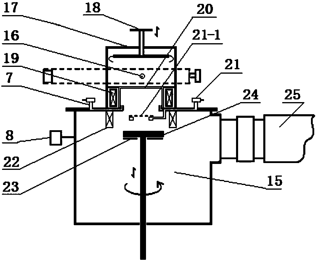
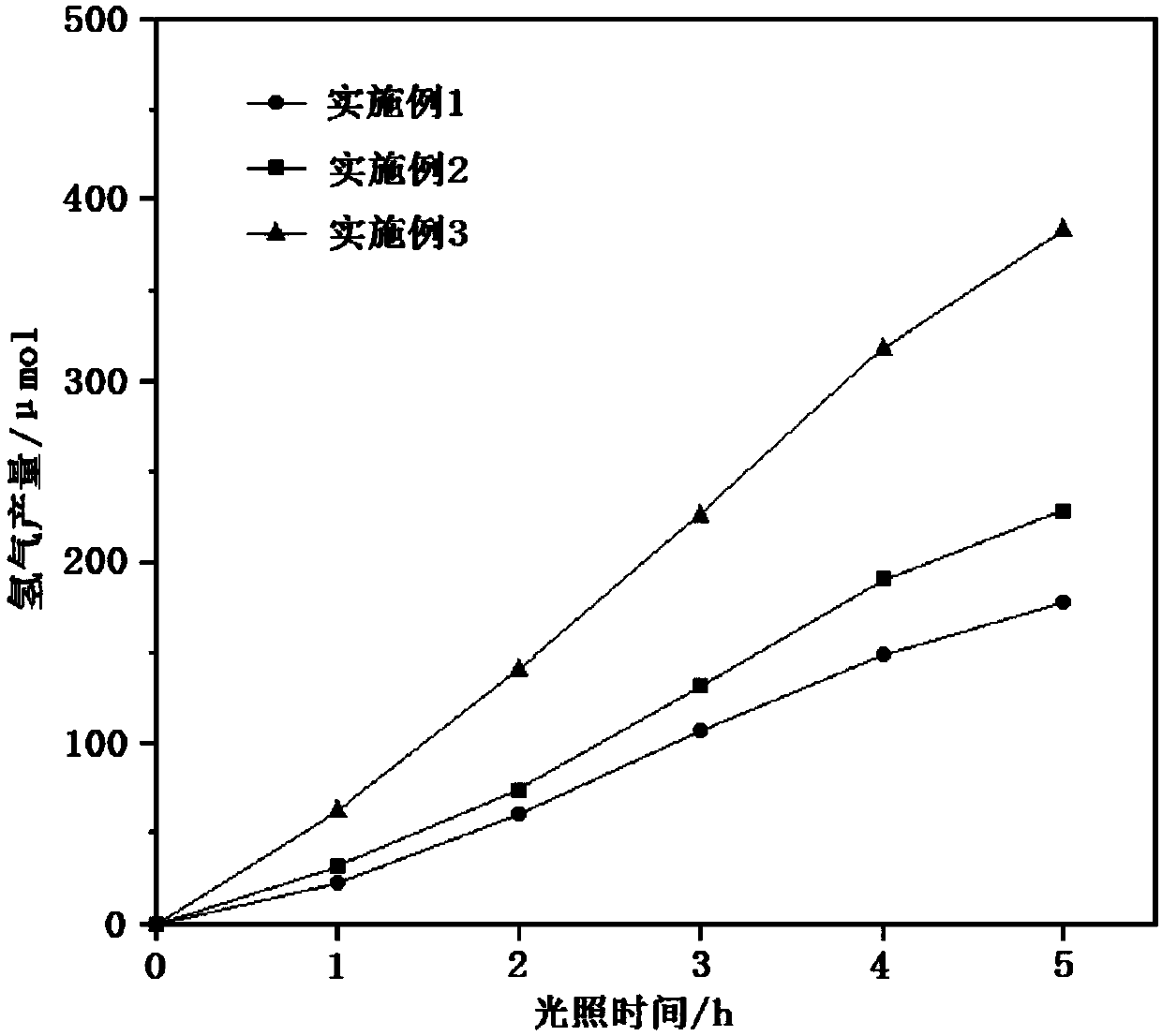
[0035] Embodiment 1, as attached figure 1 , as shown in 2, 3.
[0036] A preparation of "p-type g-C 3 N 4 / n-type Ga 0.5 Zn 0.5 N 0.5 o 0.5 "The continuous process steps of the heterogeneous PN junction visible light photocatalytic film are:
[0037] a. ECR-PEMOCVD nitriding treatment of foamed nickel-graphene composite substrate: select a commercially available foamed nickel-graphene composite substrate with a length and width of 20 mm × 20 mm, a thickness of 2 mm, a pore diameter of 50 μm, and a porosity > 97%. Substrate, this composite substrate is to be loaded with graphene layer on the framework and inner wall of nickel foam substrate, and the average thickness of graphene layer is 0.67nm; Foam nickel-graphene composite substrate, from the glove of ECR-PEMOCVD equipment The box is delivered to the sample loading room, and then from the sample loading room to the material platform 24 in the vacuum reaction chamber 15. When the background pressure of the vacuum react...
Embodiment 2
[0048] Embodiment 2, as attached figure 1 , as shown in 2, 3.
[0049] Step a-step e in embodiment 2 is exactly the same as embodiment 1, difference is: in step b and step c, ammonia flow control is 15 sccm, oxygen flow control is 18 sccm, the molar flow control of trimethylgallium TMGa 2.8×10 - 6 mol / min, the molar flow control of diethyl zinc DEZn is 7.7×10 -6 mol / min.
[0050] Using the above steps, the "p-type g-C 3 N 4 / n-type Ga 0.3 Zn 0.7 N 0.3 o 0.7 "Heterogeneous PN junction visible light photocatalytic film. Among them Ga 0.3 Zn 0.7 N 0.3 o 0.7 The thickness of the buffer layer is 20nm; n-type Ga 0.3 Zn 0.7 N 0.3 o 0.7 The layer is a columnar nanocrystalline film with c-axis preferred orientation, the film thickness is 120nm, and the silicon doping concentration is 3×10 18 cm -3 , n-type Ga 0.3 Zn 0.7 N 0.3 o 0.7 The average lateral grain size of the nanocrystals in the layer is 25.3 nm; the p-type g-C 3 N 4 The thickness of the layer is 19.5...
Embodiment 3
[0052] Embodiment 3, as attached figure 1 , as shown in 2, 3.
[0053] Step a-step e in embodiment 3 is exactly the same as embodiment 1, difference is: what step a selects for use is the commercially available length and width dimension is 20mm * 20mm, thickness is 2mm, aperture is 50 μ m, porosity > 97% Foam silver-graphene composite substrate, this composite substrate is loaded with graphene layer on the skeleton and inner wall of foam silver substrate, and the average thickness of graphene layer is 0.67nm; And in step b and step c, ammonia gas The flow control is 15 sccm, the oxygen flow control is 18 sccm, and the molar flow control of trimethylgallium TMGa is 2.8×10 -6 mol / min, the molar flow control of diethyl zinc DEZn is 7.7×10 -6 mol / min.
[0054] Using the above steps, the "p-type g-C 3 N 4 / n-type Ga 0.3 Zn 0.7 N 0.3 o 0.7 "Heterogeneous PN junction visible light photocatalytic film. Among them Ga 0.3 Zn 0.7 N 0.3 o 0.7 The thickness of the buffer laye...
PUM
| Property | Measurement | Unit |
|---|---|---|
| Thickness | aaaaa | aaaaa |
| Thickness | aaaaa | aaaaa |
| Thickness | aaaaa | aaaaa |
Abstract
Description
Claims
Application Information
 - R&D
- Intellectual Property
- Life Sciences
- Materials
- Tech Scout
- Unparalleled Data Quality
- Higher Quality Content
- 60% Fewer Hallucinations
Browse by: Latest US Patents, China's latest patents, Technical Efficacy Thesaurus, Application Domain, Technology Topic, Popular Technical Reports.
© 2025 PatSnap. All rights reserved.Legal|Privacy policy|Modern Slavery Act Transparency Statement|Sitemap|About US| Contact US: help@patsnap.com


