Thin SOI short circuit anode LIGBT

An anode and anode region technology, applied in circuits, electrical components, semiconductor devices, etc., can solve problems affecting the uniformity of current distribution of devices, and achieve the effect of suppressing the snapback effect, good compromise, and easy process compatibility.

Inactive Publication Date: 2017-10-10
UNIV OF ELECTRONICS SCI & TECH OF CHINA
View PDF4 Cites 2 Cited by
  • Summary
  • Abstract
  • Description
  • Claims
  • Application Information

AI Technical Summary

Problems solved by technology

However, the introduction of the short-circuited anode structure will bring the snapback effect to the device and affect the uniformity of the current distribution of the device.

Method used


Image

  • Thin SOI short circuit anode LIGBT
  • Thin SOI short circuit anode LIGBT
  • Thin SOI short circuit anode LIGBT

Examples


Embodiment 1

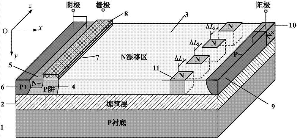
[0021] Such as figure 1 As shown, the structure of this example includes a P substrate 1, a buried oxide layer 2, and a top semiconductor layer stacked in sequence from bottom to top; along the lateral direction of the device, the top semiconductor layer is sequentially arranged from one side of the device to the other side It has a cathode structure, a P well region 4, an N drift region 3 and an anode structure; the cathode structure includes a P+ body contact region 6 and an N+ cathode region 5, and the bottom of the P+ body contact region 6 is in contact with the buried oxide layer 2, so The N+ cathode region 5 is located on the upper layer of the P well region 4, and the N+ cathode region 5 is in contact with the P+ body contact region 6 and the P well region 4, and the P+ body contact region 6 is in contact with the P well region 4; the P+ body contact region 6 and the N+ cathode The common terminal of region 5 is a cathode; the P well region 4 is in contact with the N dr...

Embodiment 2

[0025] Such as figure 2 As shown, the difference between this example and the structure of Example 1 is that the vertical spacing of the N-type islands 11 in this example is not equal, and the snapback effect can be eliminated with a smaller vertical cell size.

Embodiment 3

[0027] Such as image 3 As shown, the difference between this example and the structure of Example 1 is that in this example, the N-type islands, the P+ anode region 9 and the N+ anode region 10 are in contact with each other.


PUM


Abstract

The invention belongs to the technical field of power semiconductor, and specifically relates to a thin SOI short circuit anode LIGBT (Lateral Insulated Gate Bipolar Transistor). Compared with a traditional SOI base LIGBT, the thin SOI short circuit anode LIGBT is characterized in that an N+ anode region which is in parallel with a P+ anode region in the vertical direction, and introducing disjunctively distributed N type islands at one side, approaching a cathode structure, in the P+ anode region (9) and the N+ anode region (10); when a new device in the blockout state, the N type islands are not completely depleted, thus effectively preventing further expansion of a depletion region and preventing break-through and breakdown of the N type islands; when the initial stage is started, an electro current flows by the N type islands and the high resistance drift regions among the adjacent N type islands; and compared with traditional continuous N buffer layers, the disjunctively distributed N type islands can increase the distribution resistance at one side of the anode side to enable the device to enter the bipolar mode under a smaller current. Compared with a traditional LIGBT, the thin SOI short circuit anode LIGBT has the advantages of high speed and low on-off loss. Compared with a traditional short circuit anode LIGBT, the thin SOI short circuit anode LIGBT can eliminate the snapback effect even under a small cell size.

Description

technical field [0001] The invention belongs to the technical field of power semiconductors, and relates to a thin SOI short-circuit anode LIGBT (Lateral Insulated Gate Bipolar Transistor, lateral insulated gate bipolar transistor). Background technique [0002] As a typical representative of power electronic devices, IGBT has the advantages of high input impedance of MOSFET and low conduction voltage drop of BJT. It has unique advantages in many fields such as rail transportation, smart grid, household appliances and base stations. Due to the dielectric isolation of SOI-based LIGBT, the leakage current is reduced, the parasitic capacitance is smaller, and the radiation resistance is stronger. In addition, lateral IGBT (LIGBT) is easy to integrate, making SOI-LIGBT a core component of monolithic power integrated chips. [0003] The low turn-on voltage drop of the IGBT benefits from the conductance modulation effect in the drift region during turn-on, resulting in lower turn...

Claims


Application Information

Patent Timeline
Patent Type & Authority Applications(China)
IPC IPC(8): H01L29/06H01L29/739
CPCH01L29/0615H01L29/7394
Inventor 罗小蓉黄琳华邓高强周坤魏杰孙涛刘庆张波
Owner UNIV OF ELECTRONICS SCI & TECH OF CHINA
Why Eureka
Try Eureka