Diamond-based electrode material of seawater salinity sensor
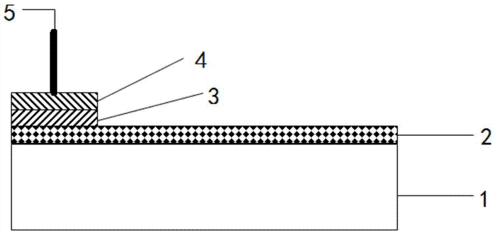
A sensor electrode, diamond technology, applied in metal material coating process, material inspection products, test water and other directions, can solve the problems affecting the measurement accuracy, reliability and life of seawater salinity sensor, electrode surface physical and chemical degradation, accuracy , reliability and life reduction, etc., to achieve the effect of strong anti-biological adhesion, strong anti-pollution characteristics, and easy reprocessing.
- Summary
- Abstract
- Description
- Claims
- Application Information
AI Technical Summary
Problems solved by technology
Method used
Image
Examples
Embodiment 1
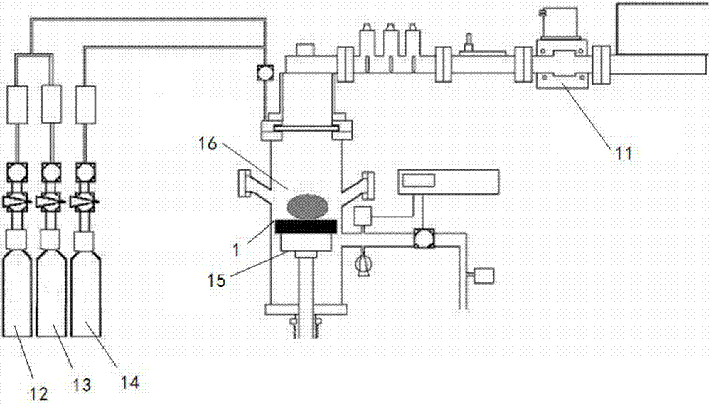
[0035] Boron-doped diamond thin film electrode materials are prepared by microwave plasma enhanced chemical vapor deposition, such as figure 2 Shown:
[0036](1) Single crystal silicon is used as the substrate 1 for depositing a boron-doped diamond film, the roughness of the silicon is 15 nm, and the thickness of the silicon wafer substrate is 400 μm. In order to achieve a high nucleation density, the monocrystalline silicon wafer was pretreated for 30 minutes in a suspension containing 0.05wt% nano-diamond particles (5nm size);
[0037] (2) The deposition process is carried out at a constant pressure of 6000Pa, the reaction temperature is 800°C, the microwave power emitted by the microwave source is 1800W, the reaction gas is a mixed gas composed of methane and hydrogen, and trimethylborane with less toxicity is added as The doped boron source realizes the growth of boron-doped nano-diamond film. The three gases are passed into the vacuum chamber 16 of the reaction chamber...
Embodiment 2
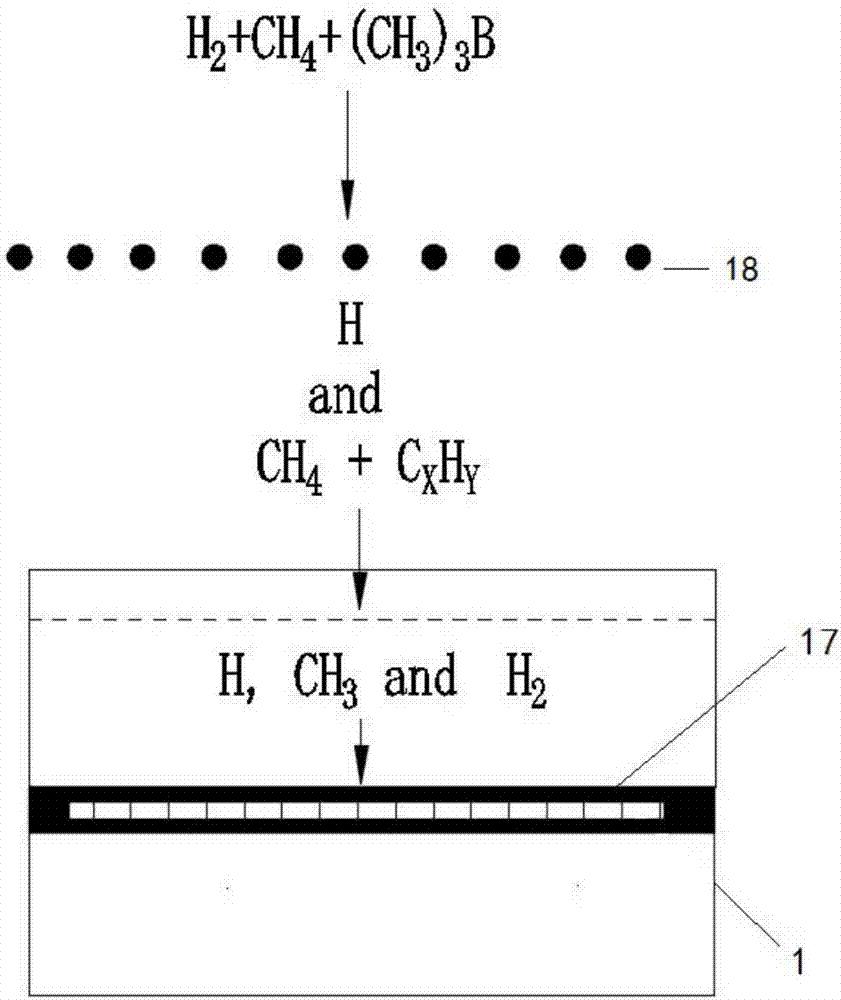
[0041] Boron-doped diamond / amorphous carbon composite thin film electrode materials are prepared by hot wire chemical vapor deposition, such as image 3 Shown:
[0042] (1) Using monocrystalline silicon as the substrate 1 for depositing the diamond composite film, the roughness of the silicon is less than 5nm, and the thickness of the silicon wafer substrate is 400 μm;
[0043] (2) Put the monocrystalline silicon substrate into the hot wire chemical vapor deposition equipment, use methane as the carbon source, trimethylborane as the boron source, and the mass concentration of boron in the mixed gas is 2000ppm, methane, hydrogen, trimethylborane The mixed gas of borane is passed into the reaction chamber, and under the action of the hot wire 18, the reaction temperature is 600 ° C, and the reaction time is 8 hours, and the boron-doped diamond / amorphous carbon with a thickness of 1 μm is prepared on the single crystal silicon substrate 1. Composite film17.
[0044] (3) A titan...
PUM
| Property | Measurement | Unit |
|---|---|---|
| Roughness | aaaaa | aaaaa |
| Thickness | aaaaa | aaaaa |
| Thickness | aaaaa | aaaaa |
Abstract
Description
Claims
Application Information
 - R&D
- Intellectual Property
- Life Sciences
- Materials
- Tech Scout
- Unparalleled Data Quality
- Higher Quality Content
- 60% Fewer Hallucinations
Browse by: Latest US Patents, China's latest patents, Technical Efficacy Thesaurus, Application Domain, Technology Topic, Popular Technical Reports.
© 2025 PatSnap. All rights reserved.Legal|Privacy policy|Modern Slavery Act Transparency Statement|Sitemap|About US| Contact US: help@patsnap.com


