Trace organic matter residue high sensitivity surface-enhanced raman detecting substrate and preparation and using method
A surface-enhanced Raman and organic technology, applied in the fields of environmental protection and spectroscopy, can solve the problems of limiting the application of SERS technology, complex synthesis process, difficult to recycle, etc., to achieve good portability, flexible and simple operation, and reduced average cost. Effect
- Summary
- Abstract
- Description
- Claims
- Application Information
AI Technical Summary
Problems solved by technology
Method used
Image
Examples
example 1
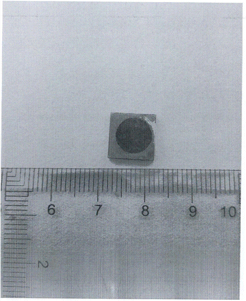
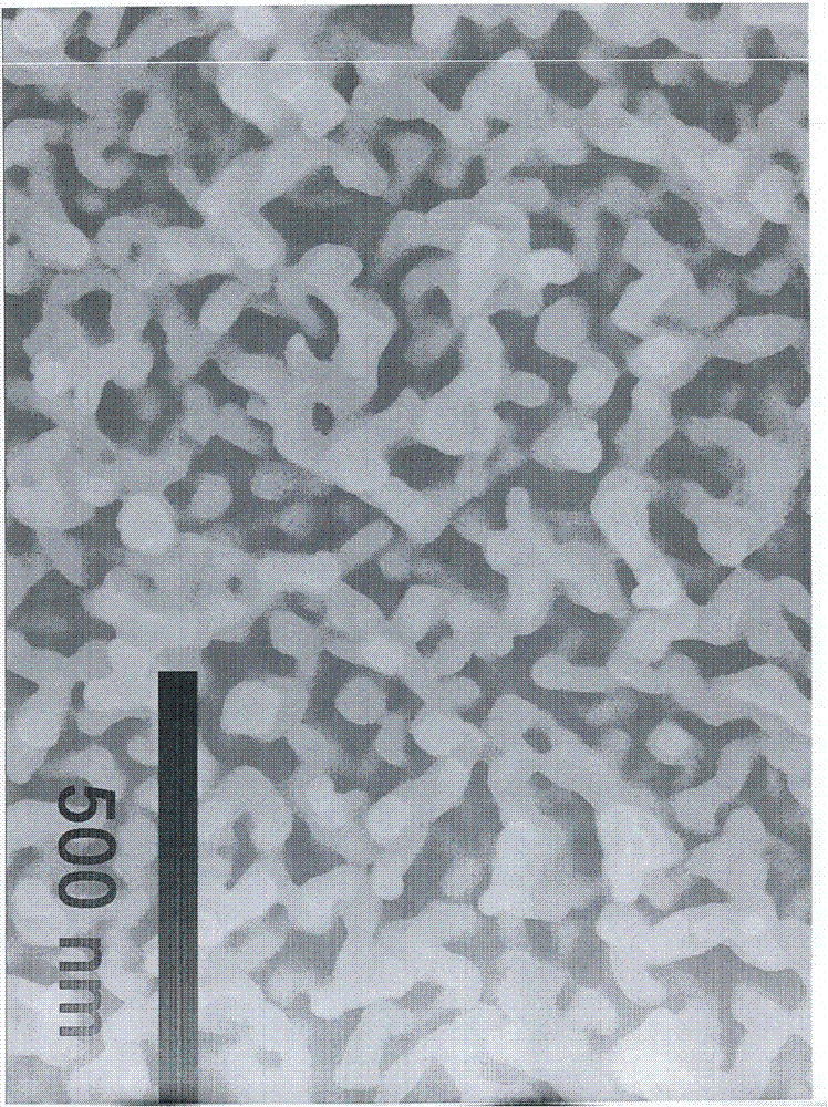
[0034] Take polycrystalline tungsten (manufactured by Xiamen Honglu Tungsten Molybdenum Technology Co., Ltd.) with a purity of 99.99wt% and a body-centered cubic (bcc) crystal structure. The size is 1cm*1cm*0.3cm, and the surface is smooth and flat by mechanical polishing; The bulk polycrystalline tungsten polished in the above steps is irradiated by a high-power plasma material irradiation experimental device. The plasma used is helium ion plasma, the ion energy is about 200Ev, and the ion current intensity is about 1.0x10 22 ions / m 2 ·s 1 , the irradiation temperature is about 1300°C, and the irradiation time is about 80 minutes. After that, a material with a nano-array morphology is formed, that is, the nano-wires grow approximately perpendicular to the planar substrate, the diameter is uniform, about 50nm, and the average spacing of the nano-wires is about 100nm, so that the bulk metal tungsten becomes a vertical array of tungsten nano-wires; On the vertically arrayed tu...
example 2
[0036] The polycrystalline tungsten (manufactured by Xiamen Honglu Tungsten Molybdenum Technology Co., Ltd.) with a purity of 99.99wt% and a body-centered cubic (bcc) crystal structure is 1cm*1cm*0.3cm in size, and its surface is smooth and flat by mechanical polishing; The bulk polycrystalline tungsten polished in the above steps is irradiated by a high-power plasma material irradiation experimental device. The plasma used is helium ion plasma, the ion energy is about 200Ev, and the ion current intensity is about 1.0x10 22 ions / m 2 ·s 1 , the irradiation temperature is about 1300°C, and the irradiation time is about 80 minutes. Afterwards, a material with a nano-array morphology is formed, that is, the nano-wires grow approximately perpendicular to the planar substrate, the diameter is uniform, about 50nm, and the average spacing of the nano-wires is about 100nm, so that the bulk metal tungsten becomes a vertical array of tungsten nano-wires; Through the Lab18 magnetron spu...
example 3
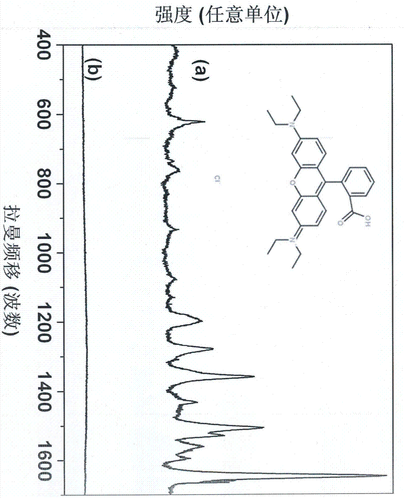
[0038] The gold-plated tungsten nanowire array obtained in Example 1 was selected as the substrate, soaked in alcohol for 1 hour, and then dried naturally for later use. Soak it in an aqueous rhodamine B solution with a concentration ranging from 10ppm to 10ppb, and let it stand at room temperature for 1 minute. The substrate soaked in the solution was taken out with tweezers, and dried naturally on filter paper for 10 minutes. After the substrate was dried, a 532nm laser was selected as the excitation light source, and a Renishaw inVia micro-Raman spectrometer was used to detect the dye molecules adsorbed on the surface of the substrate by Raman scattering at room temperature. image 3 The Raman spectrum curve shown can be compared with the Raman library to determine the composition of the sample.
PUM
 Abstract
Description
Claims
Application Information
 - R&D Engineer
- R&D Manager
- IP Professional
- Industry Leading Data Capabilities
- Powerful AI technology
- Patent DNA Extraction
Browse by: Latest US Patents, China's latest patents, Technical Efficacy Thesaurus, Application Domain, Technology Topic, Popular Technical Reports.
© 2024 PatSnap. All rights reserved.Legal|Privacy policy|Modern Slavery Act Transparency Statement|Sitemap|About US| Contact US: help@patsnap.com


