


Quick Research
Generate reliable direction feasibility study reports for your R&D in just a few steps.

Technical Q&A
Discover and master advanced knowledge NOW. Basics, ideas, possibilities, all at once.

Find Solutions
As an expert in R&D theories, this can generate solutions to your technical problems instantly.

Evaluate Feasibility
Analyze your overall solution with one click, know your potential R&D risks in advance.

Monitor Landscape
Get weekly tech updates, stay abreast of the latest tech innovations and key insights.
Switching power-semiconductor device and manufacturing method thereof
A technology of power semiconductors and manufacturing methods, which is applied in the direction of semiconductor devices, semiconductor/solid-state device manufacturing, electrical components, etc., can solve problems such as poor safe working area, high impact ionization, device leakage, etc., to improve the overall safe working area, Effect of improving conductivity and reducing on-resistance
- Summary
- Abstract
- Description
- Claims
- Application Information
AI Technical Summary
Problems solved by technology
Method used
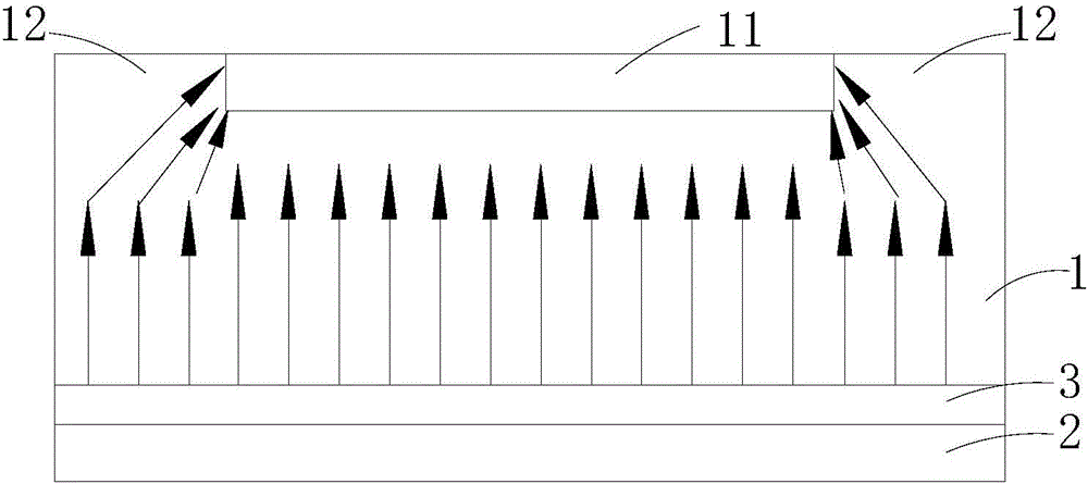
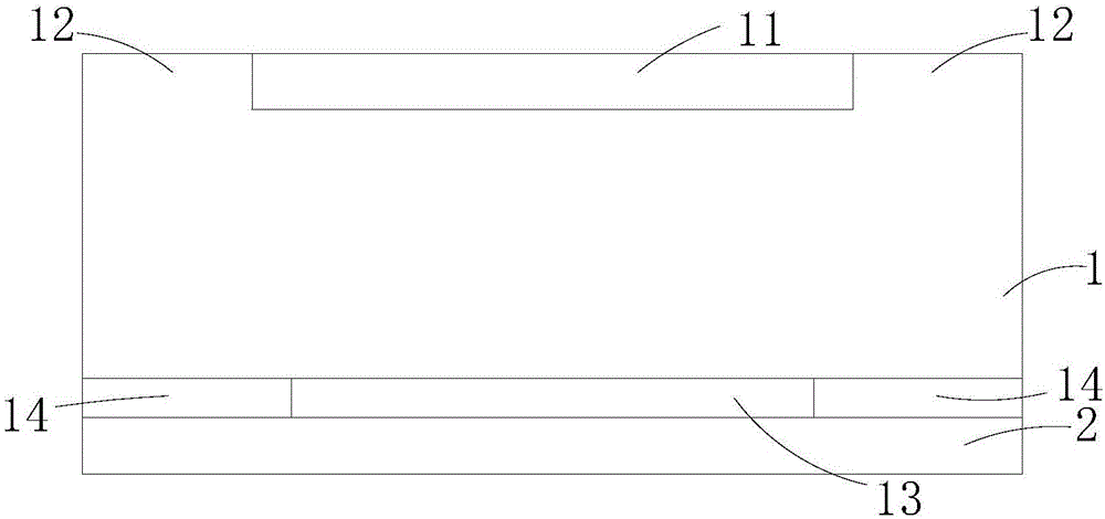
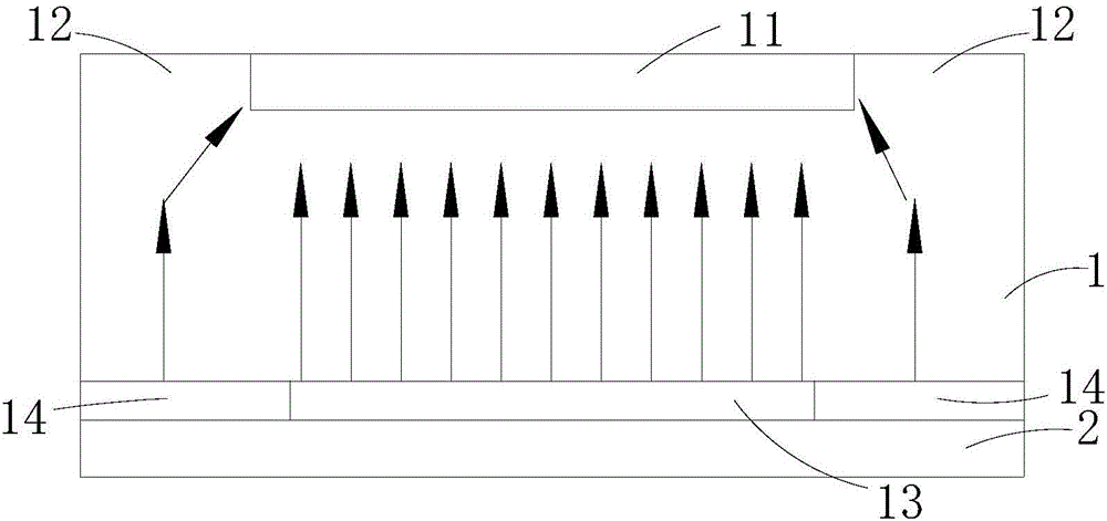
Image

Examples
Embodiment 1
[0061] A method for manufacturing a switching power semiconductor device, comprising the steps of:
[0062] 1) Select qualified semi-finished products that have completed the front process;
[0063] 2) Thinning the second surface of the semi-finished product, including first grinding and thinning the second surface, and then soaking in an aqueous sulfuric acid solution with a mass concentration of 98%. The soaking time is 10 minutes. This step of acid soaking treatment The function is to remove the silicon slag generated during grinding and remove the stress generated during grinding. Then take it out and clean it to remove the residual acid on the surface of the semi-finished product;
[0064] 3) Perform phosphorus element ion implantation to the semi-finished chip obtained in step 2), and the implantation dose is 1.0E14cm -2 ;
[0065] 4) Use laser annealing equipment to perform area-selective scanning on the second surface, and scan the center position of the second surf...
Embodiment 2
[0070] A method for manufacturing a switching power semiconductor device, comprising the steps of:
[0071] 1) Select qualified semi-finished products that have completed the front process;
[0072] 2) Thinning the second surface of the semi-finished product, including first grinding and thinning the second surface, and then soaking in an aqueous solution of nitric acid with a mass concentration of 90% and hydrofluoric acid with a mass concentration of 42%, The immersion time is 12 minutes. The role of this step of acid immersion treatment is to remove the silicon slag generated during grinding and remove the stress generated during grinding. Then take it out and clean it to remove the residual acid on the surface of the semi-finished product;
[0073] 3) Carry out boron element ion implantation to the semi-finished chip obtained in step 2), the implantation dose is 3.0E13cm -2 ;
[0074] 4) Use laser annealing equipment to perform area-selective scanning on the second surf...
PUM
 Abstract
Description
Claims
Application Information
 - R&D Engineer
- R&D Manager
- IP Professional
- Industry Leading Data Capabilities
- Powerful AI technology
- Patent DNA Extraction
Browse by: Latest US Patents, China's latest patents, Technical Efficacy Thesaurus, Application Domain, Technology Topic, Popular Technical Reports.
© 2024 PatSnap. All rights reserved.Legal|Privacy policy|Modern Slavery Act Transparency Statement|Sitemap|About US| Contact US: help@patsnap.com