Preparation method for metalized layer of copper-indium-gallium-selenium target material
A technology of copper indium gallium selenide and metallization layer, which is applied in the direction of metal material coating process, coating, and final product manufacturing, and can solve the problems of poor film thickness uniformity and composition uniformity, poor electrical and thermal conductivity, and failure to meet solar energy requirements. Battery coating process conditions and other issues, to achieve the effects of reduced production costs, low interface resistance, and good thermal conductivity
- Summary
- Abstract
- Description
- Claims
- Application Information
AI Technical Summary
Problems solved by technology
Method used
Image
Examples
Embodiment 1
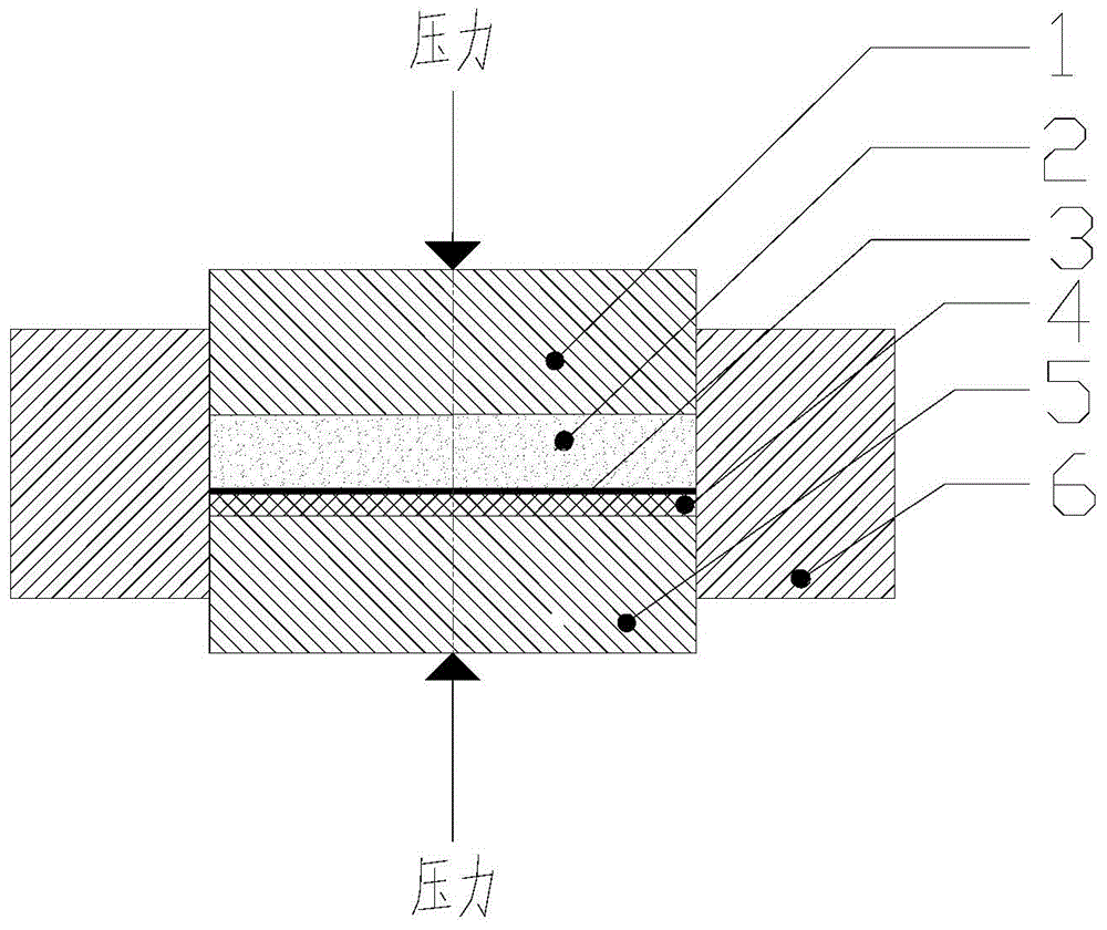
[0024] Place a graphite backing plate 4 with a thickness of 10mm on the lower pressure head 5 of the hot-press furnace mold, then place a 1mm thick Ni metal sheet 3 on the graphite backing plate 4, and then put copper indium gallium selenide powder 2, copper Indium gallium selenide powder 2 contains Cu: 25%, In+Ga: 25%, Se: 50%, and then puts it into the upper pressure head 1, and puts the mold 6 in a hot-press furnace for hot-press sintering. While raising the temperature, the pressure was gradually increased to 30 MPa, kept at a temperature of 650° C. for 60 minutes, and then cooled to room temperature. Take the target out of the hot-press furnace, firstly grind the target surface, and then grind the metallized layer, the processing amount is 0.5mm. The metallized layer and the target substrate form a metallurgical bond, and the bonding rate between the target substrate and the metallized layer is greater than 98%, which can effectively conduct heat from the target surface. ...
Embodiment 2
[0026] Place a graphite backing plate 4 with a thickness of 15mm on the lower pressure head 5 of the hot-press furnace mold, then place a 1.2mm thick Mo metal sheet 3 on the graphite backing plate 4, and then put copper indium gallium selenide powder 2, The copper indium gallium selenide powder 2 contains Cu: 25%, In+Ga: 27.5%, and Se: 47.5%, and then put it into the upper pressure head 1, and put the mold 6 in a hot-press furnace for hot-press sintering, Slowly pressurize to 40 MPa while raising the temperature, keep the temperature at 700° C. for 40 minutes, and then cool to room temperature. Take the target out of the hot-press furnace, firstly grind the target surface, and then grind the metallized layer, the processing amount is 0.7mm. The metallized layer and the target substrate form a metallurgical bond, and the bonding rate between the target substrate and the metallized layer is greater than 98.5%, which can effectively conduct heat from the target surface.
Embodiment 3
[0028] Place a graphite backing plate 4 with a thickness of 13 mm on the lower pressure head 5 of the hot-press furnace mold, then place a Cu metal sheet 3 with a thickness of 1.5 mm on the graphite backing plate 4, and then put copper indium gallium selenide powder 2, The copper indium gallium selenide powder 2 contains Cu: 25%, In+Ga: 22.5%, Se: 52.5%, and then put it into the upper pressure head 1, and put the mold 6 in a hot-press furnace for hot-press sintering, Slowly pressurize to 35 MPa while raising the temperature, keep the temperature at 680° C. for 30 minutes, and then cool to room temperature. Take the target out of the hot-press furnace, firstly grind the target surface, and then grind the metallized layer, the processing amount is 0.9mm. The metallized layer and the target substrate form a metallurgical bond, and the bonding rate between the target substrate and the metallized layer is greater than 99%, which can effectively conduct heat from the target surface....
PUM
 Abstract
Description
Claims
Application Information
 - R&D Engineer
- R&D Manager
- IP Professional
- Industry Leading Data Capabilities
- Powerful AI technology
- Patent DNA Extraction
Browse by: Latest US Patents, China's latest patents, Technical Efficacy Thesaurus, Application Domain, Technology Topic, Popular Technical Reports.
© 2024 PatSnap. All rights reserved.Legal|Privacy policy|Modern Slavery Act Transparency Statement|Sitemap|About US| Contact US: help@patsnap.com


