Hot-piercing manufacturing method of micro-via array biological chip

A technology of biochip and manufacturing method, which is applied in the direction of bioparticle analysis, chemical instruments and methods, and laboratory containers, etc., which can solve the problem of poor accuracy and speed of cancer cell morphology, inability to identify white blood cells, and greater influence on operators and other issues, to achieve the effect of low environmental requirements, controllable operation, low production process and raw material cost

Inactive Publication Date: 2016-10-12
CHONGQING INST OF GREEN & INTELLIGENT TECH CHINESE ACADEMY OF SCI
View PDF2 Cites 3 Cited by
  • Summary
  • Abstract
  • Description
  • Claims
  • Application Information

AI Technical Summary

Problems solved by technology

The accuracy and speed of observing the morphology of cancer cells by traditional optical microscope are poor, and it is greatly affected by the operator
The biochemical antigen-antibody combination method has a high misdiagnosis rate of false negatives and false positives, and consumes a large amount of high-cost auxiliary biochemical reagents. The processing process is complicated and the efficiency is low.
The existing physical microfluidic diagnosis method mainly adopts the filtering method according to the size of the cancer cells. The diagnostic efficiency is higher than the traditional method, but the accuracy is insufficient, and the mixed white blood cells cannot be identified, and the cost of the chip is relatively high, and the market price of each chip is as high as 1,000 yuan. more than yuan

Method used


Image

  • Hot-piercing manufacturing method of micro-via array biological chip
  • Hot-piercing manufacturing method of micro-via array biological chip
  • Hot-piercing manufacturing method of micro-via array biological chip

Examples


Embodiment 1

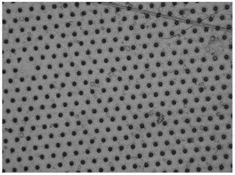
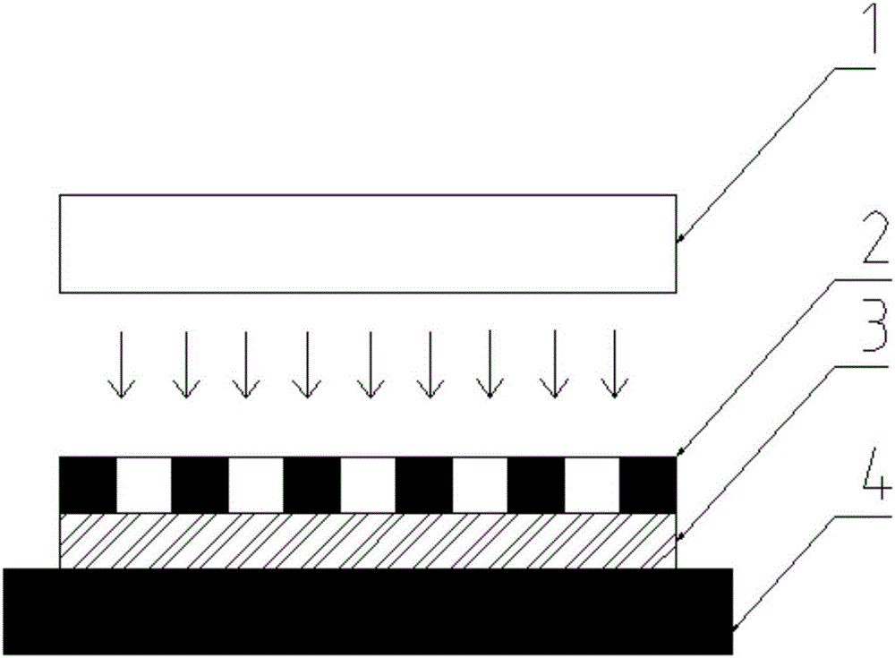
[0036] (1) The schematic diagram of the photolithography process is as follows: figure 2 As shown, the photoresist 3 is spin-coated on the quartz substrate 4, the photoresist 3 is AZ4562, the thickness of the glue is 30um, and it is baked on a hot plate at 100 degrees for 10min, and the mask plate 2 is placed on the photoresist, and the mask plate 2 The graphic is an array of microporous graphics, the micropores are circular, the pore diameter is 4um, and the ratio of the pore diameter to the gap size between the pores is 1:4. Then, it is exposed under a 365nm ultraviolet light source 1 by a contact exposure method, the exposure dose is 100mJ / cm, and it is developed for 40s, that is, the mask pattern is copied into a photoresist pattern 5 . The schematic diagram of the structure after photolithography development is as follows: image 3 shown.

[0037] (2) Configure silver ammonia solution and reducing agent solution required for chemical immersion silver. The configuratio...

Embodiment 2

[0041] (1) The schematic diagram of the photolithography process is as follows: figure 2 As shown, the photoresist 3 is spin-coated on the quartz substrate 4, the photoresist 3 is AZ50XT, the thickness of the glue is 20um, it is baked on a hot plate at 100 degrees for 10min, and the mask plate 2 is placed on the photoresist, and the mask plate 2 The pattern is an array of microporous graphics, the micropores are regular hexagons, the pore diameter is 10um, and the ratio of the pore diameter to the gap size between the pores is 1:10. Then, it is exposed under a 365nm ultraviolet light source 1 by a contact exposure method, the exposure dose is 100mJ / cm, and it is developed for 40s, that is, the mask pattern is copied into a photoresist pattern 5 . The schematic diagram of the structure after photolithography development is as follows: image 3 shown.

[0042] (2) Configure silver ammonia solution and reducing agent solution required for chemical immersion silver. The config...

Embodiment 3

[0046] (1) The schematic diagram of the photolithography process is as follows: figure 2 As shown, the photoresist 3 is spin-coated on the quartz substrate 4, the photoresist 3 is AZ50XT, the thickness of the glue is 30um, it is baked on the hot plate at 100 degrees for 10min, and the mask plate 2 is placed on the photoresist, and the mask plate 2 The graphic is an array of microporous graphics, the micropores are square, the pore diameter is 15um, and the ratio of the pore diameter to the gap size between the pores is 1:3. Then, it is exposed under a 365nm ultraviolet light source 1 by a contact exposure method, the exposure dose is 100mJ / cm, and it is developed for 40s, that is, the mask pattern is copied into a photoresist pattern 5 . The schematic diagram of the structure after photolithography development is as follows: image 3 shown.

[0047] (2) Configure silver ammonia solution and reducing agent solution required for chemical immersion silver. The configuration m...


PUM


Abstract

The invention provides a thermal piercing manufacturing method of a micro-through-hole array biological chip. The photoresist pattern is obtained by photolithography, and a metal layer is plated on the photoresist pattern by using a chemical deposition method, and then obtained by electroforming and demoulding. The original mold embryo is electrolyzed to obtain a mold, and the hot embossing method is used to pierce the polymer material through the mold to cool and demould to obtain a micro-hole array biochip. The invention adopts the hot embossing method, the equipment is easy to obtain, the requirements for the implementation environment are low, and meanwhile, the aperture periodicity and size uniformity are good, and the detection accuracy is high. The present invention realizes the controllable production of micro-through-hole array biochips made of polymer materials through the method of mold making and thermal piercing replication, greatly simplifies the processing steps, has high processing efficiency, low process cost and material cost, and is conducive to production. A high-density hole array is produced, thereby improving detection efficiency, which is very suitable for large-scale industrial production.

Description

technical field [0001] The invention belongs to the technical field of micro-nano processing methods, and in particular relates to a thermal piercing manufacturing method of a micro-hole array biochip. Background technique [0002] According to the survey results of the World Health Organization, cancer is one of the main causes of human death directly. 40% of the global annual death toll is caused by cancer, with 14 million new cancer patients and more than 8.2 million cancer deaths every year. And the number of cancer patients is increasing at a rate of close to 1.3% every year. [0003] The existing detection of blood cancer cells mainly includes microscopic examination, biochemical detection and microfluidic diagnosis. The accuracy and speed of observing the morphology of cancer cells by traditional optical microscope are poor, and it is greatly affected by the operator. The biochemical antigen-antibody combination method has a high misdiagnosis rate of false negatives...

Claims


Application Information

Patent Timeline
Patent Type & Authority Applications(China)
IPC IPC(8): B01L3/00
CPCB01L3/502707B01L3/502753B01L2200/10B01L2200/12G01N15/00G01N2015/0065
Inventor 杨勰张为国王赟姣张东张之胜夏良平史浩飞杜春雷
Owner CHONGQING INST OF GREEN & INTELLIGENT TECH CHINESE ACADEMY OF SCI
Why Eureka
Try Eureka