


Quick Research
Generate reliable direction feasibility study reports for your R&D in just a few steps.

Technical Q&A
Discover and master advanced knowledge NOW. Basics, ideas, possibilities, all at once.

Find Solutions
As an expert in R&D theories, this can generate solutions to your technical problems instantly.

Evaluate Feasibility
Analyze your overall solution with one click, know your potential R&D risks in advance.

Monitor Landscape
Get weekly tech updates, stay abreast of the latest tech innovations and key insights.
Texturing method of polycrystalline silicon wafer cut by diamond wire
A diamond wire cutting, polycrystalline silicon wafer technology, applied in the direction of polycrystalline material growth, chemical instruments and methods, crystal growth, etc., can solve the problems of unstable solution, lower reflectivity of silicon wafer, large texture fluctuation, etc., and achieve easy removal. Consistent with purification treatment, etching depth, and the effect of improving production efficiency
- Summary
- Abstract
- Description
- Claims
- Application Information
AI Technical Summary
Problems solved by technology
Method used
Image

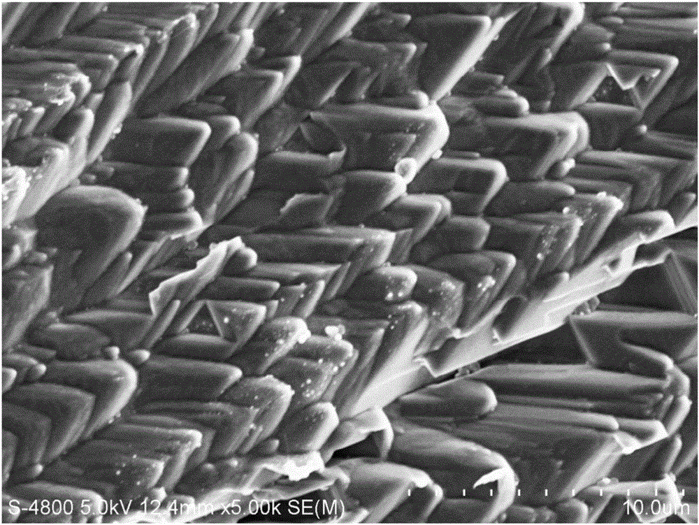
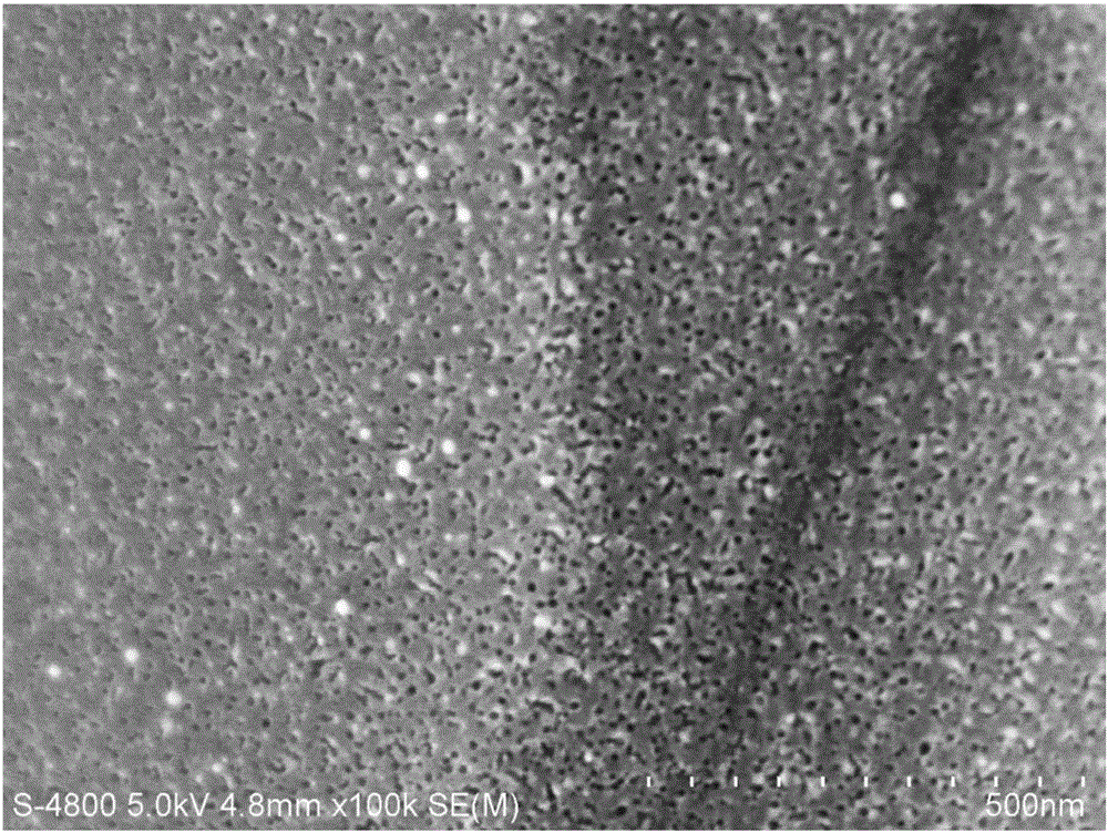
Examples
Embodiment 1
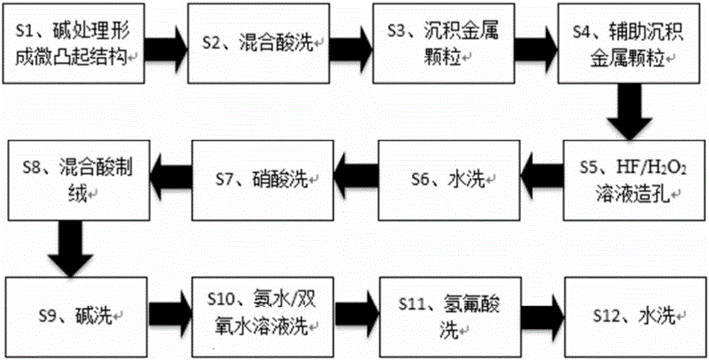
[0037] The present invention adopts the P-type 156 polysilicon wafer cut by diamond wire as the base material, and carries out the following steps of making cashmere:
[0038] (1) The cut polysilicon diamond wire slice is immersed in sodium hydroxide solution for surface treatment, and an alkali reaction control agent is added at the same time, and its concentration is 0.3%. After removing the cutting damage layer on the surface of the silicon wafer, the silicon wafer is taken out and immersed in a solution containing Cleaning is carried out in a mixed acid solution of hydrofluoric acid solution and nitric acid solution, wherein, during surface treatment, the concentration of sodium hydroxide solution is 2%, and the alkali reaction control agent is polycarboxylic acid, isooctyl alcohol polyoxyethyl ether phosphate and allyl For alcohol polyoxyalkyl ethers, the treatment temperature is 82°C, and the treatment time is 5 minutes; when cleaning, the volume ratio of hydrofluoric aci...
Embodiment 2
[0049] The basic steps are the same as in Example 1, except that the inorganic cations in step (2) are silver ions.
[0050] The reflectivity of the silicon chip sample that embodiment 1, comparative example 1 and embodiment 2 make is measured silicon chip, and above-mentioned silicon chip sample is processed as follows:
[0051] (1) Put the silicon wafer into the tubular diffusion furnace for diffusion treatment;
[0052] (2) Carry out edge etching and dephosphorous silicon glass treatment to the diffused silicon wafer;
[0053] (3) Deposit silicon nitride anti-reflection film 83nm with the method of tubular PECVD on the front after step (2) treatment;
[0054] (4) Print the back electrode and the aluminum back field on the back, and print the grid line on the front surface of the silicon wafer;
[0055] (5) Sintering to test the electrical properties of the battery sheet.
[0056] The silicon wafers prepared in embodiment 1, comparative example 1 and embodiment 2 are test...
Embodiment 3
[0066] The present invention adopts the P-type 156 polysilicon wafer cut by diamond wire as the base material, and carries out the following steps of making cashmere:
[0067] (1) Immerse the cut polysilicon diamond wire slices in sodium hydroxide solution for surface treatment, add alkali reaction control agent at the same time, its concentration is 0.1%, remove the cutting damage layer on the surface of the silicon wafer, take out the silicon wafer, and immerse it in a solution containing Cleaning is carried out in an acid solution mixed with hydrofluoric acid solution and nitric acid solution, wherein, during surface treatment, the concentration of sodium hydroxide solution is 3%, the alkali reaction control agent is polycarboxylic acid and polyethylene glycol, and the treatment temperature is 80°C. The treatment time is 5 minutes; when cleaning, the volume ratio of hydrofluoric acid and nitric acid solution is 2:1, the treatment temperature is 50°C, and the treatment time i...
PUM
| Property | Measurement | Unit |
|---|---|---|
| aperture size | aaaaa | aaaaa |
| composition ratio | aaaaa | aaaaa |
| aperture size | aaaaa | aaaaa |
Abstract
Description
Claims
Application Information
 - R&D Engineer
- R&D Manager
- IP Professional
- Industry Leading Data Capabilities
- Powerful AI technology
- Patent DNA Extraction
Browse by: Latest US Patents, China's latest patents, Technical Efficacy Thesaurus, Application Domain, Technology Topic, Popular Technical Reports.
© 2024 PatSnap. All rights reserved.Legal|Privacy policy|Modern Slavery Act Transparency Statement|Sitemap|About US| Contact US: help@patsnap.com