
Method for preparing film bulk acoustic wave resonator on the basis of monocrystal AlN

A thin-film bulk acoustic wave and resonator technology, applied in electrical components, impedance networks, etc., can solve the problems of inability to rapidly deposit single-crystal AlN thin films, bulk acoustic wave scattering, increase acoustic wave transmission loss, etc., to improve quality factor and effective electromechanical coupling. coefficient, overcoming loss, and improving the effect of crystal quality

Inactive Publication Date: 2016-06-22
FOSHAN AIFO LIGHT FLUX TECH CO LTD
View PDF6 Cites 23 Cited by
  • Summary
  • Abstract
  • Description
  • Claims
  • Application Information

AI Technical Summary

Problems solved by technology

Among them, the amorphous layer of about 5nm in the early stage of growth is beneficial to the formation of c-axis-oriented AlN thin film dendrite structure, and this layer of amorphous transition region does not contribute to piezoelectric conversion; in addition, the crystals in polycrystalline AlN Boundaries and defects can cause absorption or scattering of bulk acoustic waves, increasing acoustic wave transmission loss
Only polycrystalline AlN films with higher c-axis preferred orientation can be obtained by magnetron sputtering, but high-quality single-crystal AlN films cannot be deposited rapidly
In summary, there is still a lot of room for improvement in the performance of AlN polycrystalline films obtained by magnetron sputtering in the existing FBAR preparation process

Method used


Image

  • Method for preparing film bulk acoustic wave resonator on the basis of monocrystal AlN
  • Method for preparing film bulk acoustic wave resonator on the basis of monocrystal AlN
  • Method for preparing film bulk acoustic wave resonator on the basis of monocrystal AlN

Examples


Embodiment 1

[0029] A thin film bulk acoustic resonator based on single crystal AlN, prepared by the following preparation method:

[0030] 1. Growing the bottom electrode on the prepared substrate.

[0031] 1. Cleaning: select (111) Si substrate 1 to pass concentrated H 2 SO 4 :H 2 o 2 :H 2 O(3:1:1) and BOE:HF(20:1) cleaning to remove surface organic matter.

[0032] 2. Annealing: put the substrate at a pressure of 3.0X10 -10 In Torr's high-vacuum growth chamber, bake at 750°C for 30-60 minutes to remove pollutants on the substrate surface.

[0033] 3. Epitaxial growth of Al buffer layer: the substrate temperature is 750°C, and the Al source of MBE grows single crystal Al2 at 1050-1150°C. After 30 minutes, an Al layer is obtained with a thickness ranging from 30-300nm.

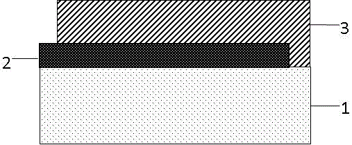
[0034] 4. Photolithography and etching the bottom electrode pattern, such as figure 1 shown.

[0035] 2. Growing a piezoelectric layer on the bottom electrode.

[0036] 5. Under the condition that the substrate ...


PUM

PropertyMeasurementUnit
Thicknessaaaaaaaaaa

Abstract

The invention discloses a method for preparing film bulk acoustic wave resonator on the basis of a monocrystal AlN. The method comprises the following steps of: growing (111) an oriented monocrystal Al film on a preparation substrate by using a molecular beam epitaxial growth method; growing (002) an oriented monocrystal AlN film on the oriented monocrystal Al film by using a pulse laser deposition growth method; and depositing a layer of metallic film on the AlN film to form a Al / AlN / metal sandwich piezoelectric stack structure. The piezoelectric stack structure based on monocrystal AlN prepared by the method can be used for preparing the film bulk acoustic wave resonator. The piezoelectric performance of the monocrystal AlN film is superior to that of a polycrystal AlN piezoelectric film applied to film bulk acoustic wave resonator so that the quality factor and a valid electromechanical coupling factor of a device are increased.

Description

technical field [0001] The invention relates to a preparation method of a thin film bulk acoustic wave resonator based on single crystal AlN. Background technique [0002] With the rapid development of wireless communication technology, more and more functional modules are required to be squeezed into the already crowded wireless terminals. Taking the mobile phone as an example, it no longer only provides basic voice communication functions, but is also compatible with a large number of digital video, camera, MP3, GPS global positioning navigation, Wi-Fi, Bluetooth and other functions. At the same time, with the development of 3G and 4G technology, the communication system tends to be more and more multi-band, showing the coexistence of multiple standards, requiring communication terminals to be able to accept each frequency band to meet the needs of different service providers and regions, which forces the mobile phone RF transceivers (RF front-ends) are developing in the ...

Claims


Application Information

Patent Timeline
IPC IPC(8): H03H3/02H03H9/17
CPCH03H3/02H03H9/171H03H9/174H03H2003/023
Inventor 李国强李洁刘国荣
Owner FOSHAN AIFO LIGHT FLUX TECH CO LTD
Learn More