Ultraviolet detector with high spectral selectivity and high sensitivity and preparation method of ultraviolet detector
An ultraviolet detector and high-sensitivity technology, applied in the field of ultraviolet detectors, can solve the problems of increasing the complexity and manufacturing cost of the detector, reducing the scope of application of the detector, and being fragile and expensive. stable effect
- Summary
- Abstract
- Description
- Claims
- Application Information
AI Technical Summary
Problems solved by technology
Method used
Image
Examples
Embodiment 1
[0029] Proceed as follows:
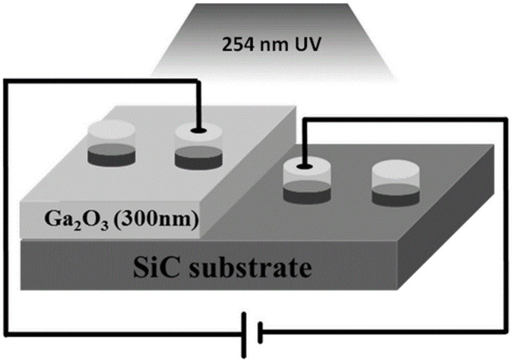
[0030] 1) Pretreatment of n-type 4H-SiC substrate: put n-type 4H-SiC substrate into V(HF):V(H 2 o 2 )=1:5 solution soaked to remove the natural oxide layer, then ultrasonic cleaning with acetone, ethanol and deionized water respectively, and vacuum drying;
[0031] 2) Place the target and substrate: place the Ga 2 o 3 The target is placed on the target stage of the laser molecular beam epitaxy system, and the n-type 4H-SiC substrate processed in step 1) is fixed on the sample holder and put into the vacuum chamber;
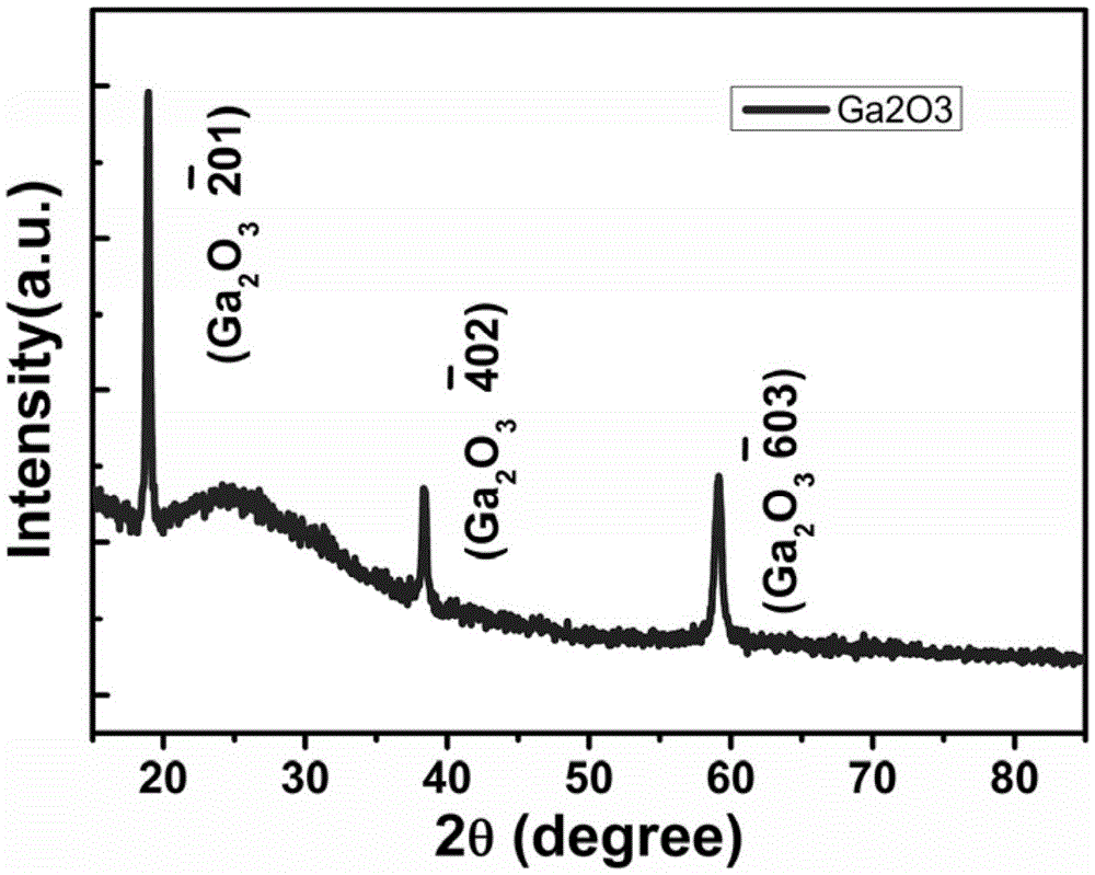
[0032] 3) β-Ga 2 o 3 Thin film deposition process: first vacuumize the chamber, feed oxygen, adjust the pressure in the vacuum chamber, heat the n-type 4H-SiC substrate, and grow β-Ga 2 o 3 thin film, after the growth of the thin film is completed, continue to feed oxygen, adjust the pressure in the vacuum chamber, and the obtained β-Ga 2 o 3 The thin film is annealed in situ; among them, Ga 2 o 3 The distance between the ta...
Embodiment 2
[0037] Steps (1), (2) and (4) are all the same as in Example 1. In step (3), the chamber is first evacuated, oxygen is introduced, the pressure in the vacuum chamber is adjusted, and the n-type 4H-SiC substrate is heated to grow β-Ga 2 o 3 thin film, after the growth of the thin film is completed, continue to feed oxygen, adjust the pressure in the vacuum chamber, and the obtained β-Ga 2 o 3 The thin film is annealed in situ; among them, Ga 2 o 3 The distance between the target and the n-type 4H-SiC substrate was set at 5 cm, and the chamber pressure after vacuuming was 1×10 -6 Pa, when heating the n-type 4H-SiC substrate, the cavity pressure is 1×10 -3 Pa, β-Ga 2 o 3 When the film is annealed in situ, the cavity pressure is 1Pa, and the laser energy is 200mJ / cm 2 , the laser pulse frequency is 1Hz, the laser wavelength is 248nm, the heating temperature of n-type 4H-SiC substrate is 700℃, β-Ga 2 o 3 The annealing temperature of the film is 700° C., and the annealing ...
Embodiment 3
[0040] Steps (1), (2) and (4) are all the same as in Example 1. In step (3), the chamber is first evacuated, oxygen is introduced, the pressure in the vacuum chamber is adjusted, and the n-type 4H-SiC substrate is heated to grow β-Ga 2 o 3 thin film, after the growth of the thin film is completed, continue to feed oxygen, adjust the pressure in the vacuum chamber, and the obtained β-Ga 2 o 3 The thin film is annealed in situ; among them, Ga 2 o 3 The distance between the target and the n-type 4H-SiC substrate was set at 5 cm, and the chamber pressure after vacuuming was 1×10 -6 Pa, when heating the n-type 4H-SiC substrate, the cavity pressure is 1×10 -3 Pa, β-Ga 2 o 3 When the film is annealed in situ, the cavity pressure is 1.5Pa, and the laser energy is 200mJ / cm 2 , the laser pulse frequency is 1Hz, the laser wavelength is 248nm, the heating temperature of n-type 4H-SiC substrate is 750℃, β-Ga 2 o 3 The annealing temperature of the film is 700° C., and the annealin...
PUM
 Abstract
Description
Claims
Application Information
 - R&D
- Intellectual Property
- Life Sciences
- Materials
- Tech Scout
- Unparalleled Data Quality
- Higher Quality Content
- 60% Fewer Hallucinations
Browse by: Latest US Patents, China's latest patents, Technical Efficacy Thesaurus, Application Domain, Technology Topic, Popular Technical Reports.
© 2025 PatSnap. All rights reserved.Legal|Privacy policy|Modern Slavery Act Transparency Statement|Sitemap|About US| Contact US: help@patsnap.com


