
Electrochemical treatment method for surface etching of absorption layer of copper zinc tin sulfide thin film solar cell

A thin-film solar cell, copper-zinc-tin-sulfur technology, applied in the field of solar cells, can solve the problems of serious environmental pollution and high cost, and achieve the effects of overcoming unenvironmental protection, reducing recombination rate, and improving roughness

Active Publication Date: 2016-06-01
CHENGDU SCI & TECH DEV CENT CHINA ACAD OF ENG PHYSICS
View PDF5 Cites 3 Cited by
  • Summary
  • Abstract
  • Description
  • Claims
  • Application Information

AI Technical Summary

Problems solved by technology

[0008] The main purpose of the present invention is to provide an electrochemical treatment method for etching the surface of the absorbing layer of a copper-zinc-tin-sulfur thin film solar cell in view of the deficiencies of the prior art, serious environmental pollution and high cost

Method used


Image

  • Electrochemical treatment method for surface etching of absorption layer of copper zinc tin sulfide thin film solar cell
  • Electrochemical treatment method for surface etching of absorption layer of copper zinc tin sulfide thin film solar cell
  • Electrochemical treatment method for surface etching of absorption layer of copper zinc tin sulfide thin film solar cell

Examples


Embodiment 1

[0043] Embodiment 1 This embodiment is an electrochemical method to etch the surface of the copper-zinc-tin-sulfur film

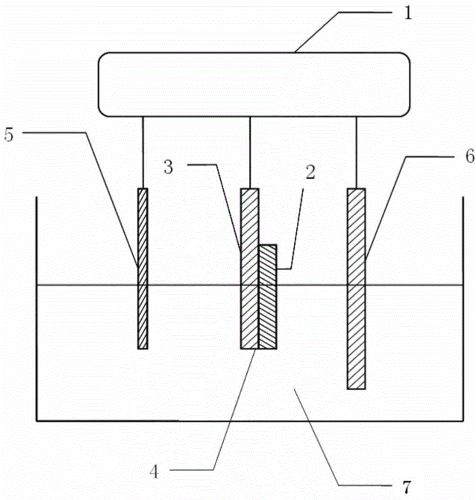
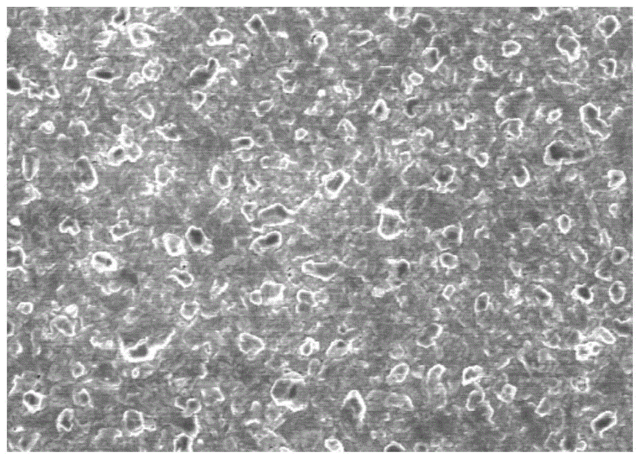
[0044] Metal Mo with a thickness of 1 μm is deposited on the soda-lime glass, and a copper-zinc-tin-sulfur thin film 2 with a thickness of 1-2 μm is deposited on the Mo layer 4 by electrochemical deposition, and then annealed in a quartz tube furnace. The scanning electron microscope picture of the CuZnSnS thin film 2 after selenization is shown in figure 2 .

[0045] Step (1): connect the selenized copper-zinc-tin-sulfur thin film 2 to the working electrode of the electrochemical workstation 1, the connecting part is only the Mo layer 4, soak it in absolute ethanol solution for 1 to 2 minutes, remove the surface stained with particulate impurities;

[0046] Step (2): preparation treatment solution 7, treatment solution 7 is the mixed solution of potassium sulfite, potassium sulfide and deionized water, the concentration of potassium sulfite in the mixed...

Embodiment 2

[0049] Embodiment 2 This embodiment is an electrochemical method to etch the surface of the copper-zinc-tin-sulfur film

[0050] Metal Mo with a thickness of 1 μm is deposited on soda-lime glass, and a copper-zinc-tin-sulfur thin film 2 with a thickness of 1-2 μm is deposited on the Mo layer 4 by pulse electrochemical deposition, and then annealed in a quartz tube furnace.

[0051] Step (1): connect the selenized copper-zinc-tin-sulfur thin film 2 to the working electrode of the electrochemical workstation 1, the connecting part is only the Mo layer 4, soak it in absolute ethanol solution for 1 to 2 minutes, remove the surface stained with particulate impurities;

[0052] Step (2): Prepare treatment solution 7, treatment solution 7 is a mixed solution of sodium sulfite, sodium sulfide and deionized water, the concentration of sodium sulfite in the mixed solution is 0.25M / L, and the concentration of sodium sulfide in the mixed solution is 0.35M / L, pH=13;

[0053] Step (3): P...

Embodiment 3

[0055] Embodiment 3 This embodiment is an electrochemical method to etch the surface of the copper-zinc-tin-sulfur film

[0056] Metal Mo with a thickness of 1 μm is deposited on soda-lime glass, and a copper-zinc-tin-sulfur thin film 2 with a thickness of 1-2 μm is deposited on the Mo layer 4 by pulse electrochemical deposition, and then annealed in a quartz tube furnace.

[0057] Step (1): connect the selenized copper-zinc-tin-sulfur thin film 2 to the working electrode of the electrochemical workstation 1, the connecting part is only the Mo layer 4, soak it in absolute ethanol solution for 1 to 2 minutes, remove the surface stained with particulate impurities;

[0058] Step (2): preparation treatment solution 7, treatment solution 7 is the mixed solution of potassium sulfite, sodium sulfide and deionized water, the concentration of potassium sulfite in the mixed solution is 0.25M / L, the concentration of sodium sulfide in the mixed solution The concentration is 0.35M / L, pH=...


PUM


Abstract

The invention relates to the technical field of solar cells, and specifically discloses an electrochemical treatment method for surface etching of an absorption layer of a copper zinc tin sulfide thin film solar cell. The method includes the steps of: placing a copper zinc tin sulfide thin film in an electrochemical workstation after selenylation or sulfuration, only connecting a Mo layer with a working electrode, soaking in absolute ethyl alcohol to remove particle impurities; preparing a treatment solution which is a mixed solution of sulfite, metal sulfide and deionized water and whose pH value is 8 to 14; applying an electrical signal, taking the copper zinc tin sulfide thin film out after 1 to 600 seconds, using deionized water to wash the thin film, and drying the thin film with high-purity nitrogen, the electrical signal being any one of a cyclic voltammetry electrical signal, a constant voltage electrical signal, a constant current electrical signal, a pulse voltage electrical signal or a pulse current electrical signal. The method provided by the invention can effectively dissolve a harmful secondary phase protruding from the surface of the thin film, etches defects of the surface of the thin film, reduces the recombination rate of photon-generated carrier pairs at an interface, is environment-friendly, and facilitates industrial popularization.

Description

technical field [0001] The invention belongs to the technical field of solar cells, in particular to an electrochemical treatment method for etching the surface of an absorbing layer of a copper-zinc-tin-sulfur thin film solar cell. Background technique [0002] Solar energy is the most abundant energy among many renewable energy sources. The energy of global sunlight for one hour is equivalent to the energy consumption of the earth for a year, which is much higher than wind energy, geothermal energy, hydropower, ocean energy, biomass energy and other energy sources. The proportion of solar energy in the future energy structure will increase, and it is conservatively estimated that this proportion will exceed 60% in 2100. Therefore, solar cell research is an important topic for future energy development. [0003] Copper zinc tin sulfur (CuZn x sn y S z , can also include selenium Se, abbreviated as CZTS) is a derivative of copper indium gallium selenium CIGS, the crystal...

Claims


Application Information

Patent Timeline
IPC IPC(8): H01L31/18C25F3/14
CPCY02P70/50
Inventor 何绪林张永政廖成刘江叶勤燕梅军刘焕明
Owner CHENGDU SCI & TECH DEV CENT CHINA ACAD OF ENG PHYSICS
Learn More