Copper selenide hollow tubular multi-stage structure material as well as preparation method and application thereof
A structural material, copper selenide technology, applied in electrical components, electrolytic capacitors, capacitors and other directions, can solve the problems of cumbersome synthesis steps, less research on copper selenide, poor stability, etc., and achieve the effect of simple preparation steps
- Summary
- Abstract
- Description
- Claims
- Application Information
AI Technical Summary
Problems solved by technology
Method used
Image
Examples
Embodiment 1
[0039] a Cu 2-X The preparation method of Se nanocrystalline counter electrode material, its step is as follows:
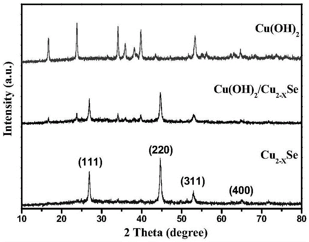
[0040] First, polish the copper foil with sandpaper, wash the FTO and the copper foil with decontamination powder, then use acetone, 95% ethanol, and secondary deionized water to ultrasonically wash for 20 minutes, and then vacuum dry. At room temperature, soak the copper foil (3.0cm*2.5cm) in a solution containing sodium hydroxide aqueous solution (10M, 8.0mL), ammonium persulfate aqueous solution (1.0M, 4mL), ammonia dilute solution (25%, 4mL), two in a mixture of deionized water (40.0 mL). React for 45 minutes, rinse with secondary water and 95% ethanol in turn, and dry in vacuum. Then, soak it in 0.01 mol / L solution and react for 30 minutes (selenization time). Finally, soak it in 20% ammonia water dilute solution and react for 8 hours. Rinse with secondary water and 95% ethanol in sequence, and dry in vacuum.
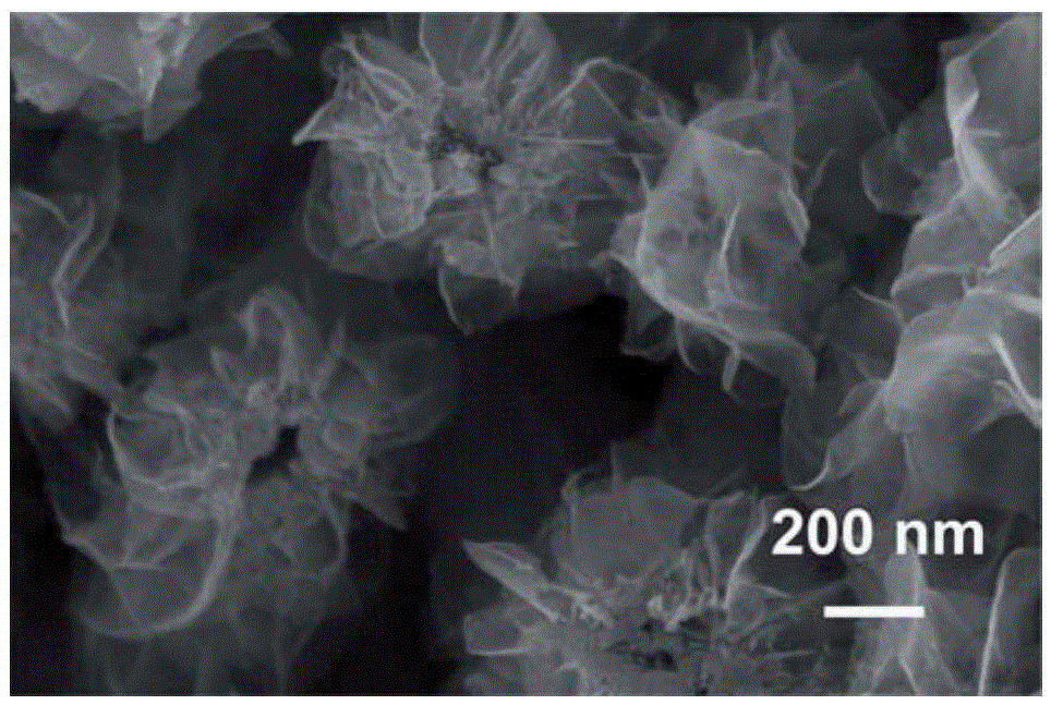
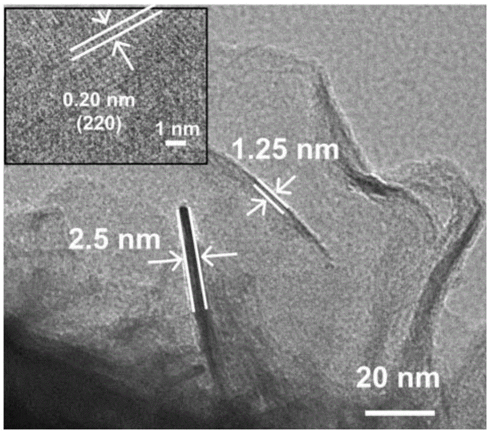
[0041] figure 1 is the X-ray diffraction s...
Embodiment 2
[0043] The steps are the same as in Example 1, except that the selenium ion concentration in Example 1 is changed to 0.005 mol / liter. Figure 4 Respectively, the transmission diagram of the product obtained in Example 2, reducing the concentration of the reaction solution, the displacement reaction rate decreases, the reaction is not carried out completely, Cu(OH) 2 Cu grown on the upper end of the rod-like structure 2-X The Se nanosheets are smaller, with a thickness of 3.14–3.57 nm, and their specific surface areas are 15.67 m 2 g -1 .
Embodiment 3
[0045] The steps are the same as in Example 1, except that the selenium ion concentration in Example 1 is changed to 0.02 mol / liter. Figure 5 Respectively, the transmission diagrams of the products obtained in Example 3. However, the morphology of the lower end of the rod-like structure does not change significantly. As the concentration increases, the displacement reaction rate accelerates, and the Cu 2-X The Se nanosheets become significantly larger, and since the reaction rate is greater than the downward migration rate of Se ions, the upper end of the rod-like structure grows larger relative to the lower end. The thickness of the nanosheet is 4.75-6.25nm, and its specific surface area is 41.76m 2 g -1 .
PUM
| Property | Measurement | Unit |
|---|---|---|
| diameter | aaaaa | aaaaa |
| diameter | aaaaa | aaaaa |
| thickness | aaaaa | aaaaa |
Abstract
Description
Claims
Application Information
 - R&D
- Intellectual Property
- Life Sciences
- Materials
- Tech Scout
- Unparalleled Data Quality
- Higher Quality Content
- 60% Fewer Hallucinations
Browse by: Latest US Patents, China's latest patents, Technical Efficacy Thesaurus, Application Domain, Technology Topic, Popular Technical Reports.
© 2025 PatSnap. All rights reserved.Legal|Privacy policy|Modern Slavery Act Transparency Statement|Sitemap|About US| Contact US: help@patsnap.com


