Drive control device
A technology of drive control and gate drive, which is applied in the field of drive control devices and can solve problems such as reduction of conduction loss
- Summary
- Abstract
- Description
- Claims
- Application Information
AI Technical Summary
Problems solved by technology
Method used
Image
Examples
no. 1 Embodiment approach
[0083] Below, refer to Figure 1 to Figure 5 A first embodiment of the present application will be described. figure 1 The drive control system shown is used in a power conversion device such as an inverter device that drives an inductive load such as a motor, and a converter device that includes an inductor to step up or step down a DC voltage. Semiconductor elements 1A and 1B as switching elements are arranged in series between the DC power supply line 2 on the high potential side and the DC power supply line 3 on the low potential side with the output terminal Nt interposed therebetween to form a half bridge circuit 4 .
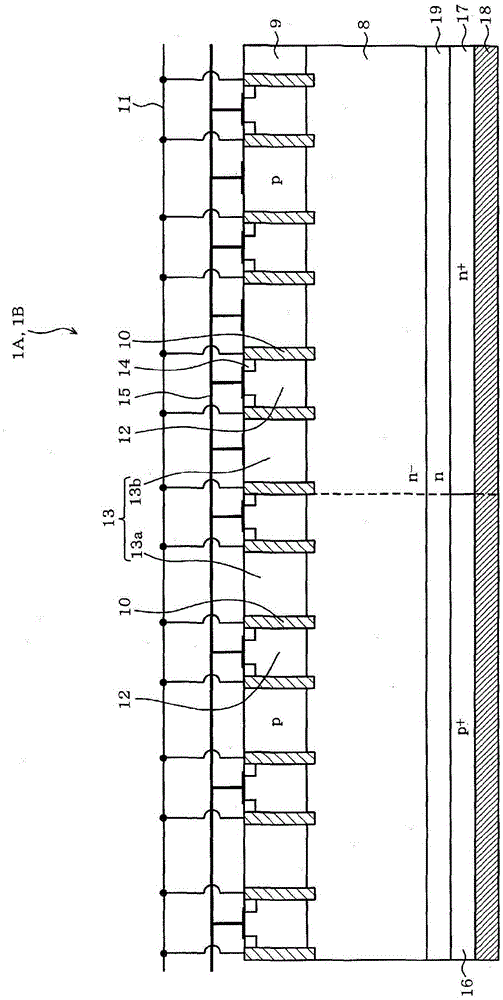
[0084] The semiconductor elements 1A and 1B having the same structure are reverse conduction IGBTs (RC-IGBTs) in which an insulated gate type transistor element 5 and a diode element 6 are formed on the same semiconductor substrate. The energization electrodes (collector, emitter) of the transistor element 5 and the energization electrodes (cathode, anod...
no. 2 Embodiment approach
[0127] For the second embodiment using MOS transistors in the semiconductor elements 1A and 1B, refer to Image 6 and Figure 7 Be explained. The structure of the drive control device 32A, 32B is figure 1as shown. Here, the operation of the low-side drive control device 32B will be mainly described. The function of the drive control device 32A on the high side is also the same.
[0128] When using MOS transistors as the semiconductor elements 1A and 1B, the switching signal Sk is switched to H level, for example. The drive control device 32B sets the current threshold It based on the threshold voltage Vt input from the threshold setting circuit 29B, and executes Vf control.
[0129] Image 6 is a voltage-current characteristic diagram when a current flows in the forward direction of the diode element 6 in the MOS transistor. The magnitude relationship between the forward voltage Vf of the diode element 6 when the gate drive voltage is cut off and the drain-source volta...
Embodiment approach
[0202] Figure 20 Showing the twelfth embodiment, Figure 21 The thirteenth embodiment is shown, and drive control devices 152 and 154 using drive ICs 151 and 153 both having a high withstand voltage are shown. The high withstand voltage refers to a withstand voltage corresponding to the power supply voltage applied to the half-bridge circuit 4 . The drive control devices 152 and 154 drive and control the two semiconductor elements 101A and 101B constituting the half-bridge circuit 4 .
[0203] The drive ICs 151 and 153 include a common Vf control unit 26 and a common pulse control unit 27 for the semiconductor elements 101A and 101B, and operate when supplied with a power supply voltage VDD (for example, 15V). The gate drive signal SGH is given to the semiconductor element 101A via the level shifter 57 and the drive circuit 28 , and the gate drive signal SGL is given to the semiconductor element 101B via the drive circuit 28 .
[0204] Drive IC 151 includes voltage detecti...
PUM
 Abstract
Description
Claims
Application Information
 - R&D Engineer
- R&D Manager
- IP Professional
- Industry Leading Data Capabilities
- Powerful AI technology
- Patent DNA Extraction
Browse by: Latest US Patents, China's latest patents, Technical Efficacy Thesaurus, Application Domain, Technology Topic, Popular Technical Reports.
© 2024 PatSnap. All rights reserved.Legal|Privacy policy|Modern Slavery Act Transparency Statement|Sitemap|About US| Contact US: help@patsnap.com


