
Low reflectivity solar crystalline silicon cell and manufacturing method thereof

A solar cell, low reflectivity technology, applied in the field of solar cells, can solve the problems of polluted environment, silicon wafer damage, high fragmentation rate, and achieve the effects of eliminating mechanical damage, avoiding surface damage, and improving conversion efficiency

Inactive Publication Date: 2015-12-30
GUANGDONG AIKO SOLAR ENERGY TECH CO LTD
View PDF7 Cites 1 Cited by
  • Summary
  • Abstract
  • Description
  • Claims
  • Application Information

AI Technical Summary

Problems solved by technology

At present, due to the remarkable effect of nano-velvet in reducing reflectivity, it has become one of the most important methods for preparing high-efficiency solar cells. Dry etching and wet etching technologies have appeared, but this technology has many disadvantages : The cost of dry etching is high, the damage to the silicon wafer is serious, and the fragmentation rate is high; the wet etching solution seriously pollutes the environment

Method used


Image

  • Low reflectivity solar crystalline silicon cell and manufacturing method thereof

Examples


Embodiment Construction

[0018] In order to make the object, technical solution and advantages of the present invention clearer, the present invention will be further described in detail below in conjunction with the accompanying drawings.

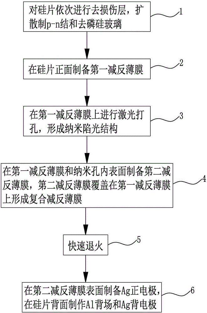
[0019] Such as figure 1 Shown, a kind of preparation method of low reflectivity crystalline silicon solar cell comprises the steps:

[0020] Step 1: Carry out the damage removal layer on the silicon wafer in sequence, diffuse the p-n junction and remove the phosphorus-silicate glass. The damage removal layer is to corrode a layer of 1-5 μm silicon damage layer on the surface of the silicon wafer by acid or alkali.

[0021] Step 2: Prepare the first anti-reflection film on the front side of the silicon wafer.

[0022] Step 3: Carry out laser drilling on the first anti-reflection film to form a nano-light trapping structure; the first anti-reflection film is a silicon nitride film with a thickness of 60-75nm and a refractive index of 2.05-2.10; the nano-light trapp...


PUM

PropertyMeasurementUnit
thicknessaaaaaaaaaa
diameteraaaaaaaaaa
thicknessaaaaaaaaaa

Abstract

The invention discloses a low reflectivity solar crystalline silicon cell and a manufacturing method thereof. The method comprises steps that, a), a damaged layer of a silicon chip is sequentially removed, and a p-n knot and dephosphorization silicon glass are prepared through expansion; b), a first anti-reflection film is prepared at the front face of the silicon chip; c), laser punching is carried out on the first anti-reflection film to form a nano light tripping structure; d), a second anti-reflection film is prepared on the surface of the first anti-reflection film and in a nano hole, and the second anti-reflection film covers the first anti-reflection film to form a composite anti-reflection film; e), rapid annealing is carried out; and f), a Ag positive electrode is prepared on the surface of the second anti-reflection film, and an Al back field and a Ag back electrode are prepared on the back face of the silicon chip. Compared with the prior art, the method is advantaged in that, the surface of the crystalline silicon is prevented from being damaged, a carrier composition rate on the silicon surface is reduced, reflectivity is reduced, and cell conversion efficiency is improved. The invention further discloses the low reflectivity solar crystalline silicon cell prepared through the manufacturing method.

Description

technical field [0001] The invention relates to the technical field of solar cells, in particular to a low-reflectivity crystalline silicon solar cell and a preparation method thereof. Background technique [0002] The loss of photoelectric conversion efficiency of crystalline silicon solar cells has various forms, including: optical loss, resistance heat loss and electron-hole recombination loss, among which optical loss is one of the important obstacles hindering the improvement of solar cell efficiency. For crystalline silicon, the band gap is about 1.12eV, and the corresponding intrinsic absorption wavelength is 1.1 μm, that is, photons with a wavelength greater than 1.1 μm cannot be used and lost. In addition, near-infrared or red light with a longer wavelength, due to its small absorption coefficient, is generally not absorbed until it is close to the back surface of the battery, and even needs to be reflected back into the silicon wafer through the back to be absorbed...

Claims


Application Information

Patent Timeline
Patent Type & Authority Applications(China)
IPC IPC(8): H01L31/18H01L31/0216H01L31/068
CPCH01L31/02168H01L31/068H01L31/1804H01L31/1868Y02E10/547Y02P70/50
Inventor 石强秦崇德方结彬黄玉平何达能陈刚
Owner GUANGDONG AIKO SOLAR ENERGY TECH CO LTD
Learn More