Automatic solder mask exposure frame module and exposure machine

A technology of exposure tables and frame molds, which is applied in microlithography exposure equipment, photolithography exposure devices, optics, etc., and can solve problems affecting product quality, low efficiency, and insufficient adsorption

Active Publication Date: 2017-06-23
龙岩海圣科技有限公司
View PDF4 Cites 0 Cited by
  • Summary
  • Abstract
  • Description
  • Claims
  • Application Information

AI Technical Summary

Problems solved by technology

[0003] In the traditional technology, the direct contact between the upper and lower glass will lead to insufficient adsorption of each part, and when the vacuum is pumped, due to the direct contact between the circuit board and the film, it may press out the imprint of the film, affecting the quality of the product and increasing the defect rate.
[0004] In addition, the fully automatic double-sided exposure machines currently on the market, in essence, add automatic flipping and alignment devices inside the single-sided exposure machine, which is not true double-sided simultaneous exposure, resulting in high cost and low efficiency. Shortcomings
At present, the main reason why double-sided simultaneous exposure cannot be implemented is that automatic alignment is not possible, because in the solder mask exposure process, the surface of the circuit board is coated with ink. Viscosity, after placing the circuit board between the upper and lower glass plates, it is basically impossible to move and align

Method used


Image

  • Automatic solder mask exposure frame module and exposure machine
  • Automatic solder mask exposure frame module and exposure machine
  • Automatic solder mask exposure frame module and exposure machine

Examples


Embodiment 1

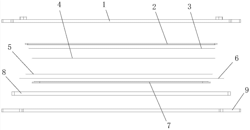
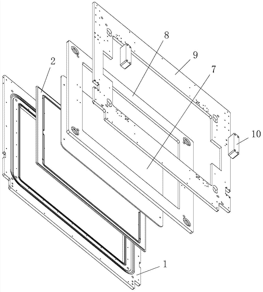
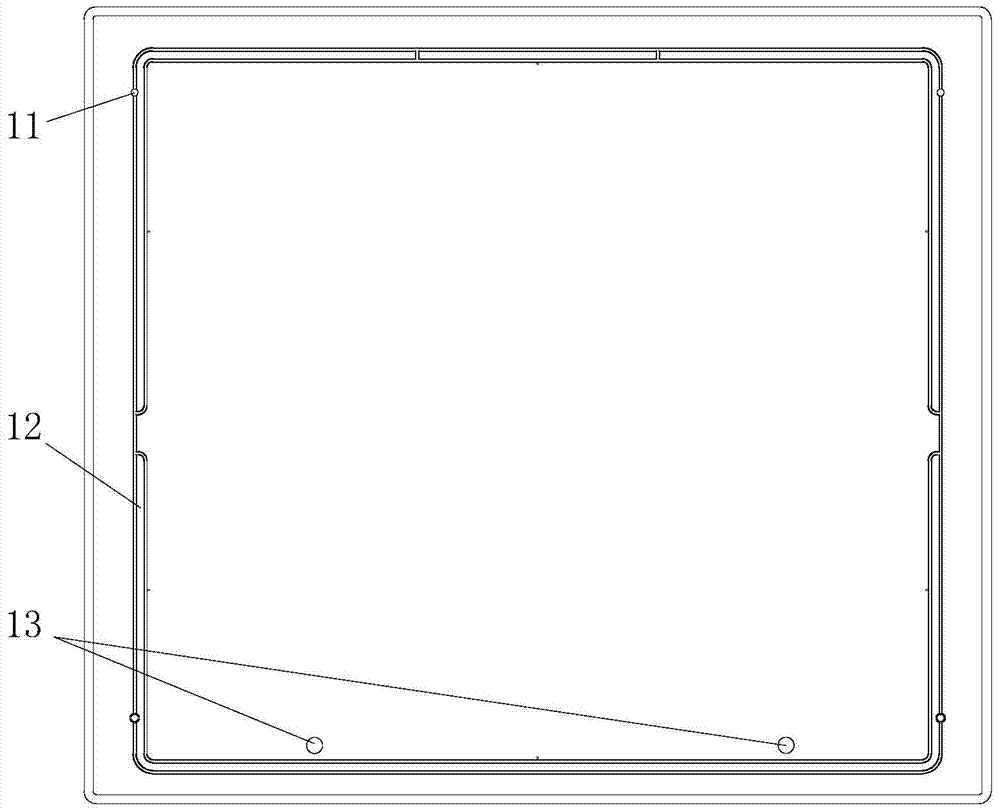
[0029] Embodiment 1, for automatic double-sided exposure, refer to figure 1 , figure 2 , image 3 , Figure 4 with Figure 5 , the automatic solder mask exposure table frame module and the exposure machine, the table frame module is installed in the host 14 of the automatic solder mask exposure machine, the host 14 is connected with a control mechanism 15, the host 14 has an alignment platform 18, an optical alignment Device 17 (such as a CCD lens), frame module 16, exposure chamber 20, exposure light source and power supply mechanism, frame module 16 is installed in the host 14, and the transfer mechanism in the host 14 exposes the frame module 16 The transfer inside and outside the chamber 20; the exposure light source exposes the circuit boards in the frame module transferred to the exposure chamber; the alignment platform 18 and the optical alignment device 17 cooperate to align the circuit boards in the frame module; The table frame module includes an upper frame 1, ...

Embodiment 2

[0044] Embodiment 2 is used for automatic single-sided exposure. The difference from automatic double-sided exposure is that only the lower glass 7 and the lower negative film 5 need to be removed, and the step of alignment between the circuit board 4 and the lower negative film 5 is omitted.


PUM


Abstract

The invention discloses an automatic solder-mask exposure table frame module and an exposure machine. The table frame module comprises an upper frame, upper glass, an upper negative plate, a circuit board, a lower negative plate (existing during double-sided exposure), a film medium, lower glass (double-sided exposure), a movable frame and a lower frame, wherein the movable frame is built on the lower frame; the lower glass is embedded into the movable frame; the film medium sleeves the lower glass and is embedded into the movable frame; the lower negative plate is put on the film medium; the upper negative plate is arranged on the circuit board; the upper glass is located above the upper negative plate; the upper frame is arranged above the upper glass; and various components have vacuum absorption structures. The automatic solder-mask exposure table frame module can be applied to automatic single-sided exposure and automatic double-sided exposure; positioning is carried out through the movable frame by supporting the circuit board; and the film medium is added between the circuit board (or the lower negative plate) and the lower glass, so that the capacity can be improved by 60%-80%. Due to the film medium, imprints of the negative plates can be prevented from being pressed on the circuit board during vacuum supply; the exposure accuracy can be improved when a glass plate is uneven or the circuit board warps; and the reject ratio is reduced.

Description

technical field [0001] The invention relates to the technical field of processing and manufacturing of electronic circuit boards, in particular to a module mechanism, an exposure machine and an alignment method in the circuit board solder mask exposure technology. Background technique [0002] With the development of electronic technology, the application of circuit boards (PCB / FPC, etc.) is becoming more and more extensive, and the technical requirements for its processing and manufacturing are getting higher and higher. Usually, circuit board exposure is an important process in the circuit board manufacturing process, which is divided into three cases: inner layer exposure, outer layer exposure and solder mask exposure. [0003] In the traditional technology, the direct contact between the upper and lower glass will lead to insufficient adsorption of each part, and when the vacuum is pumped, due to the direct contact between the circuit board and the film, it may press out...

Claims


Application Information

Patent Timeline
Patent Type & Authority Patents(China)
IPC IPC(8): G03F7/20G03F9/00
Inventor 袁强刘长征唐绍亮
Owner 龙岩海圣科技有限公司
Why Eureka
Try Eureka