A kind of silicon carbide surface treatment method
A surface treatment, silicon carbide technology, applied in electrical components, semiconductor/solid-state device manufacturing, circuits, etc., can solve the problems of poor controllability, high equipment requirements, and high use costs, and achieve low cost and good controllability.
- Summary
- Abstract
- Description
- Claims
- Application Information
AI Technical Summary
Problems solved by technology
Method used
Image

Examples
Embodiment 1
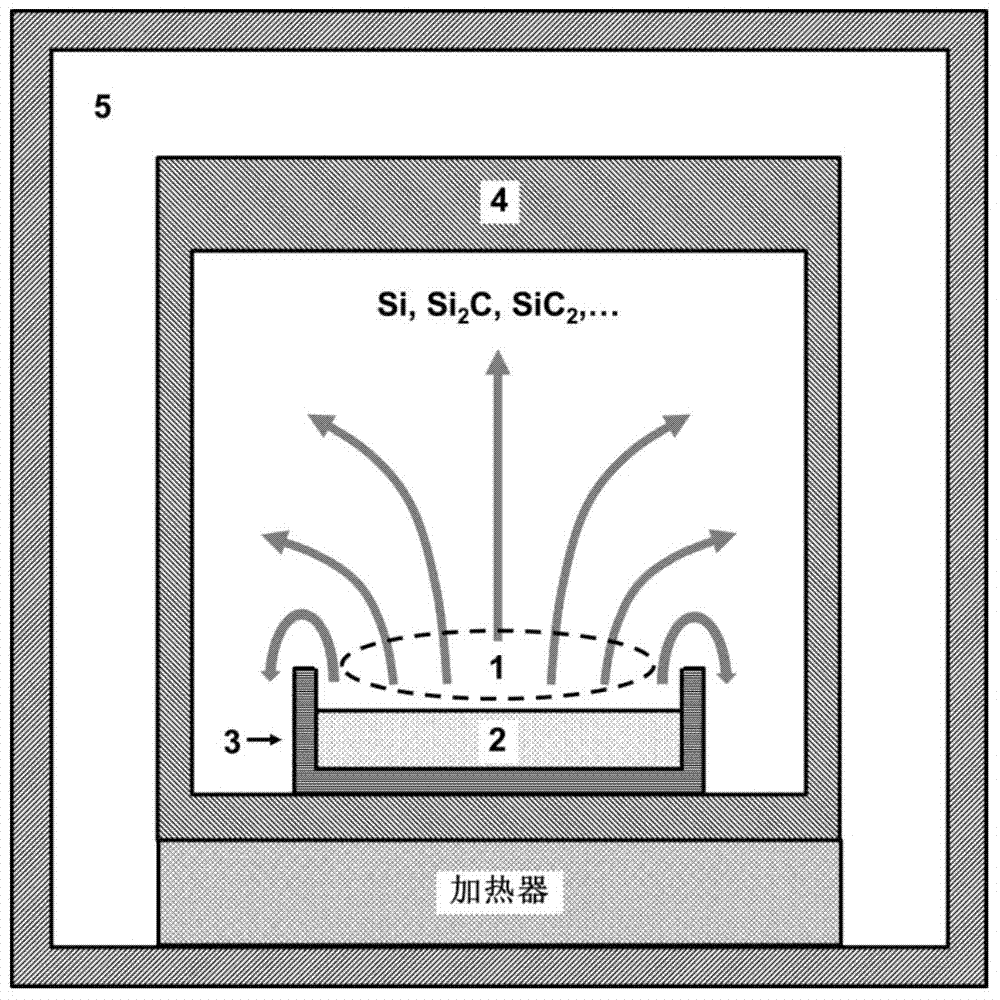
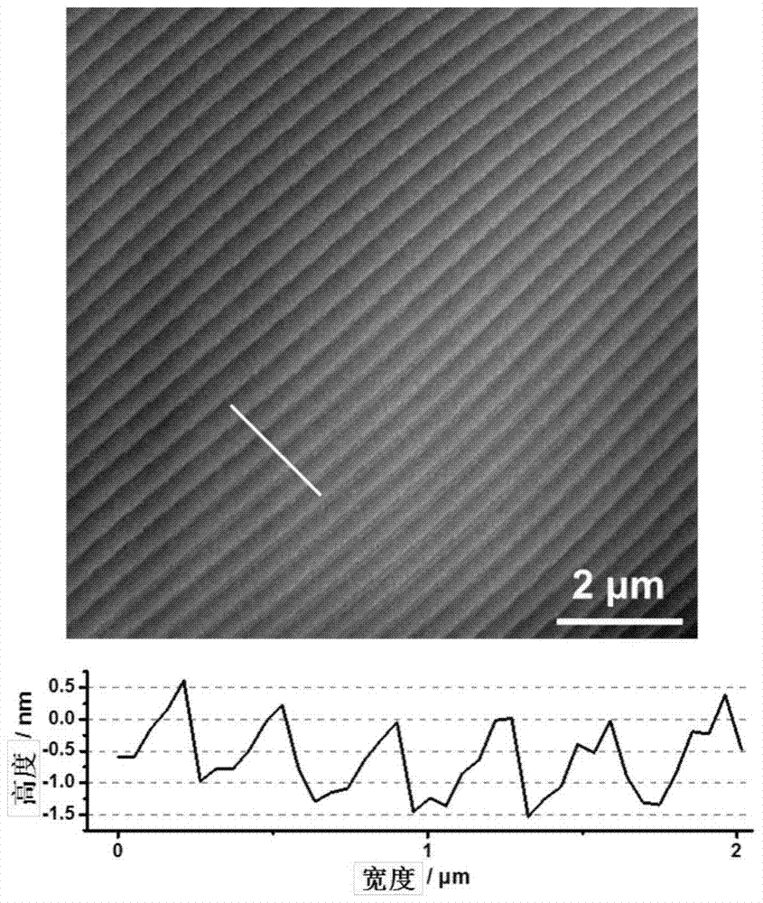
[0029] This embodiment provides a silicon carbide surface treatment method, as follows figure 2 The method is described in detail. The silicon carbide surface treatment method provided in this embodiment includes the following steps:
[0030] 1) Provide a 6H-SiC(000-1) silicon carbide wafer 1 of 2×2 square centimeters. Under normal temperature and normal pressure, the silicon carbide wafer 1 is ultrasonically cleaned with acetone and absolute ethanol in sequence, and cleaned with deionized water. , to remove the organic matter on the surface of the silicon carbide wafer 1 . Then use dilute hydrochloric acid, dilute hydrofluoric acid for further ultrasonic cleaning, and clean with deionized water to remove metal impurities and silicon dioxide oxide layer on the surface of silicon carbide wafer 1 . Finally, the cleaned silicon carbide wafer 1 is blown dry with nitrogen.
[0031] 2) Evenly put silicon carbide powder 2 with an average particle size of about 5 microns into the ...
Embodiment 2
[0037] This embodiment provides a silicon carbide surface treatment method, comprising the following steps:
[0038] 1) Provide a 4H-SiC(000-1) silicon carbide wafer 1 of 3×3 square centimeters. Under normal temperature and normal pressure, the silicon carbide wafer 1 is ultrasonically cleaned with acetone and absolute ethanol in sequence, and cleaned with deionized water , to remove the organic matter on the surface of the silicon carbide wafer 1 . Then use dilute hydrochloric acid, dilute hydrofluoric acid for further ultrasonic cleaning, and clean with deionized water to remove metal impurities and silicon dioxide oxide layer on the surface of silicon carbide wafer 1 . Finally, the cleaned silicon carbide wafer 1 is blown dry with nitrogen.
[0039] 2) Evenly put silicon carbide powder 2 with an average particle size of about 10 microns into the WC crucible 3 to ensure that the filling thickness of the silicon carbide powder 2 in the WC crucible 3 exceeds 1 mm, and then pu...
Embodiment 3
[0044] This embodiment provides a silicon carbide surface treatment method, as follows Figure 5 The method is described in detail. The silicon carbide surface treatment method provided in this embodiment includes the following steps:
[0045] 1) A 2-inch 6H-SiC (0001) silicon carbide wafer 21 is provided, and the silicon carbide wafer 21 is ultrasonically cleaned with acetone and absolute ethanol in sequence at room temperature and pressure, and cleaned with deionized water to remove silicon carbide Organic matter on the surface of the wafer 21. Then use dilute hydrochloric acid, dilute hydrofluoric acid for further ultrasonic cleaning, and clean with deionized water to remove metal impurities and silicon dioxide oxide layer on the surface of silicon carbide wafer 21 . Finally, the cleaned silicon carbide wafer 21 is blown dry with nitrogen.
[0046] 2) Evenly fill the silicon carbide powder 22 with an average particle size of about 20 microns into the graphite crucible 24...
PUM
| Property | Measurement | Unit |
|---|---|---|
| particle size | aaaaa | aaaaa |
Abstract
Description
Claims
Application Information
 - R&D
- Intellectual Property
- Life Sciences
- Materials
- Tech Scout
- Unparalleled Data Quality
- Higher Quality Content
- 60% Fewer Hallucinations
Browse by: Latest US Patents, China's latest patents, Technical Efficacy Thesaurus, Application Domain, Technology Topic, Popular Technical Reports.
© 2025 PatSnap. All rights reserved.Legal|Privacy policy|Modern Slavery Act Transparency Statement|Sitemap|About US| Contact US: help@patsnap.com