Charge pump circuit of charge transfer structure suitable for low-voltage operation

A charge pump and low-voltage technology, which is applied in the field of semiconductor integrated circuits, can solve problems such as large layout area, and achieve the effects of simple layout design, improved conduction capability, and low power consumption

Inactive Publication Date: 2015-08-05
GIANTEC SEMICON LTD
View PDF2 Cites 4 Cited by
  • Summary
  • Abstract
  • Description
  • Claims
  • Application Information

AI Technical Summary

Problems solved by technology

M0 and M3 are used in parallel in the circuit and need to occupy a larger layout area

Method used


Image

  • Charge pump circuit of charge transfer structure suitable for low-voltage operation
  • Charge pump circuit of charge transfer structure suitable for low-voltage operation
  • Charge pump circuit of charge transfer structure suitable for low-voltage operation

Examples


Embodiment Construction

[0025] For the technical means that the present invention realizes, feature and effect are easy to understand, combine below Figure 4 and Figure 5 for further clarification. These descriptions and illustrations of embodiments should not be construed as limitations of the present invention. Obvious changes to the characteristics of the examples of the present invention and the extension of its application principles will also fall within the protection scope of the present invention.

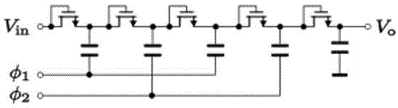
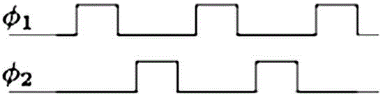
[0026] A charge pump circuit provided by the present invention is a further improvement to the improved Dickson charge pump circuit called CTS, which can provide the required operating voltage for non-volatile memory integrated circuits, such as being used in EEPROM or flash memory chips, with low Voltage operation to generate the high voltage required for programming and erasing.

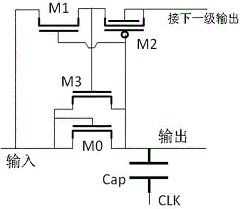
[0027] The CTS charge pump circuit suitable for low-voltage operation provided by the present invention includ...


PUM


Abstract

The invention relates to a charge pump circuit of a charge transfer structure CTS suitable for low-voltage operation. The charge pump circuit comprises a plurality of cascaded CTS charge pump sub-units. Each stage of CTS charge pump sub-unit comprises the components of a first NMOS transistor as a transmission switch, the drain electrode of the first NMOS transistor is connected with the input end of this stage, and the source electrode is connected with the output end of this stage; a second NMOS transistor of which the drain electrode is connected with the input end of this stage, the source electrode is connected with the gate electrode of the first NMOS transistor, and the gate electrode is connected with the output end of this stage; a PMOS transistor of which the source electrode is connected with the gate electrode of the first NMOS transistor, the drain electrode is connected with the output end of a next stage, and the gate electrode is connected with the output end of this stage; and a random phase clock signal in a pair of phase clock signals, wherein the random phase clock signal is transmitted to the output end of this stage through an energy storage lifting capacitor. The charge pump circuit is based on the improvement of the existing CTS charge pump sub-unit and a cascaded circuit, and increases the gate electrode voltage of the NMOS transistor as a transmission switch through a simpler structure. Furthermore the charge pump circuit has functions of reducing side effect of a substrate bias effect and simplifying design for a circuit board diagram.

Description

technical field [0001] The invention relates to a semiconductor integrated circuit, in particular to a charge pump circuit for generating high voltage in an EEPROM (Electrically Erasable Programmable Read-Only Memory, Electrically Erasable Programmable Read-Only Memory) or a flash memory chip. Background technique [0002] With the rise of handheld devices and the Internet of Things, the demand for integrated circuit miniaturization and energy-saving design is becoming more and more urgent, which puts forward requirements for the design of low power supply voltage of semiconductor integrated circuits. Because EEPROM and flash memory devices have the characteristics of flexible data rewriting, stored data content will not be lost after power failure, and can be kept for a long time, they are more and more widely used in the system. [0003] In CMOS EEPROM or flash memory devices, whether based on floating gate technology or charge trap technology, a high voltage generation ci...

Claims


Application Information

Patent Timeline
IPC IPC(8): H02M3/07
CPCH02M3/07
Inventor 袁庆鹏
Owner GIANTEC SEMICON LTD
Why Eureka
Try Eureka