Chip Separation Method for 3D Stacked Chip Packaging Devices
A technology of chip packaging and separation method, which is applied in semiconductor/solid-state device manufacturing, semiconductor/solid-state device testing/measurement, electrical components, etc. Electrical measurement analysis, avoidance of inclined grinding damage, and the effect of smooth grinding surface
- Summary
- Abstract
- Description
- Claims
- Application Information
AI Technical Summary
Problems solved by technology
Method used
Image
Examples
Embodiment 1
[0038] In this embodiment, the memory containing two chips of NAND Flash+Mobile SDRAM (the two-layer chips adopt the form of cross-stacking) is taken as an example, and the second layer of chips is obtained by separation. The separation method includes the following steps (for the technical flow chart, see figure 1 ):
[0039] (1) Determine the grinding area and its area
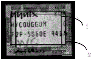
[0040] Scanning Acoustic Microscopy (C-SAM) memory internal structure such as figure 2 As shown, the memory is a cross-type double-sided lead package, in which, 1 is the first layer chip, and 2 is the second layer chip; the packaging material and 1 the first layer chip are determined to be the grinding area, and the area is 8mm; at the same time, the memory initial The thickness is about 1mm. According to experience, usually the uppermost packaging material accounts for about 1 / 3 of the total thickness of the memory, which provides a reference for the grinding force when grinding the packaging material in ...
PUM
 Abstract
Description
Claims
Application Information
 - Generate Ideas
- Intellectual Property
- Life Sciences
- Materials
- Tech Scout
- Unparalleled Data Quality
- Higher Quality Content
- 60% Fewer Hallucinations
Browse by: Latest US Patents, China's latest patents, Technical Efficacy Thesaurus, Application Domain, Technology Topic, Popular Technical Reports.
© 2025 PatSnap. All rights reserved.Legal|Privacy policy|Modern Slavery Act Transparency Statement|Sitemap|About US| Contact US: help@patsnap.com


