


Quick Research
Generate reliable direction feasibility study reports for your R&D in just a few steps.

Technical Q&A
Discover and master advanced knowledge NOW. Basics, ideas, possibilities, all at once.

Find Solutions
As an expert in R&D theories, this can generate solutions to your technical problems instantly.

Evaluate Feasibility
Analyze your overall solution with one click, know your potential R&D risks in advance.

Monitor Landscape
Get weekly tech updates, stay abreast of the latest tech innovations and key insights.
Back contact layer structure and CdTe solar battery comprising back contact layer structure
A solar cell, back contact technology, applied in circuits, photovoltaic power generation, electrical components, etc., can solve problems such as large diffusion coefficient and battery performance degradation
- Summary
- Abstract
- Description
- Claims
- Application Information
AI Technical Summary
Problems solved by technology
Method used
Image

Examples
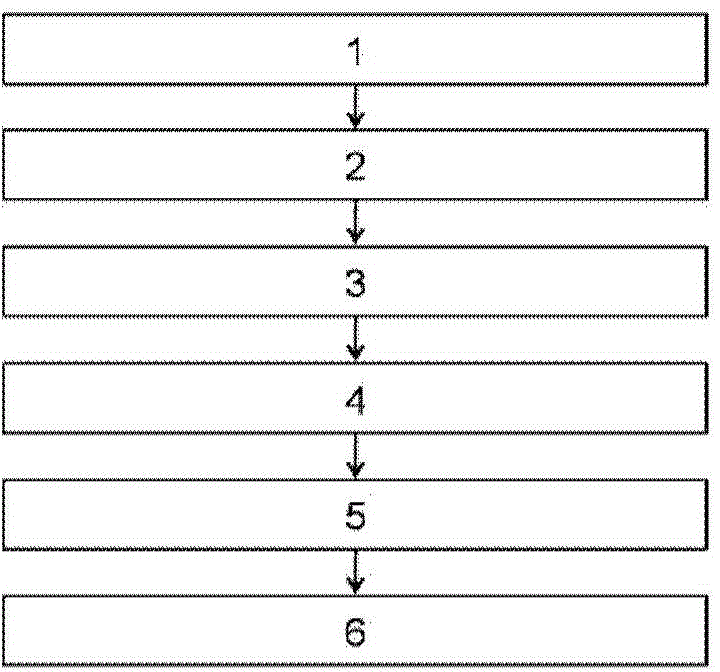
Embodiment approach 1
[0041] (1) Chemical etching of CdTe surface
[0042] Put the surface-cleaned glass / transparent conductive film / cadmium sulfide / cadmium telluride thin film structure sample into phosphoric acid nitric acid solution (volume ratio: nitric acid: phosphoric acid: water = 1:70:29) and etch for 5 to 50 seconds, etch After finishing, the sample surface was rinsed with deionized water, and then blown dry with N2.
[0043] (2) Deposition of Cu metal film
[0044] Put the etched sample into the vacuum chamber with a vacuum degree of 5×10 -6 Pa, using the electron beam evaporation method, deposited a 2nm thick Cu metal layer on the surface of the sample.
[0045] (3) Deposition V 2 o 5 film
[0046] The deposited Cu film samples were placed in the vacuum chamber of the magnetron sputtering instrument, and V 2 o 5 film. In the background vacuum (5×10 -3 Pa) under the condition, feed oxygen and argon into the system at the same time. The magnetron sputtering atmosphere is a mixed ...
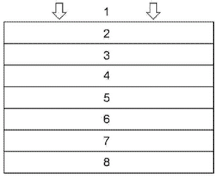
Embodiment approach 2
[0048] (1) Chemical etching of CdTe surface
[0049] Put the glass / transparent conductive film / cadmium sulfide / cadmium telluride film structure sample with clean surface into bromine methanol solution (the volume ratio of bromine to methanol is 1:1000) and etch for 5 to 50 seconds, and use The surface of the sample was rinsed with deionized water and then washed with N 2 blow dry.
[0050] (2) Deposition of Cu metal film
[0051] Put the etched sample into the vacuum chamber with a vacuum degree of 5×10 -6 Pa, using the electron beam evaporation method to deposit a 1nm thick Cu metal layer on the surface of the sample.
[0052] (3) Deposition of MoO 3 film
[0053] Put the deposited Cu film sample into the vacuum chamber of the magnetron sputtering instrument, and use 4N pure MoO 3 Preparation of MoO by radio frequency sputtering on the target 3 film. In the background vacuum (5×10 -3 Pa) under the condition, feed oxygen and argon into the system at the same time. Th...
Embodiment approach 3
[0055] (1) Dry etching of CdTe surface
[0056] Place the glass / transparent conductive film / cadmium sulfide / cadmium telluride film structure sample with clean surface in vacuum (5×10 -3 Pa) conditions, using plasma beam (argon ion) bombardment method to remove excess CdCl on the surface 2 and oxides produced during heat treatment. The process is carried out in a pure argon atmosphere of 0.2-0.4Pa, and the bombardment power and beam current are related to the size of the sample area. The bombardment time is about 10 minutes.
[0057] (2) Deposition of Cu metal film
[0058] Put the etched glass / TCO / CdS / CdTe into a vacuum chamber with a vacuum degree of 5×10 -6 Pa, using the electron beam evaporation method, deposited a 1nm thick Cu metal layer on the surface of the sample.
[0059] (3) Deposition V 2 o 5 film
[0060] The sample of deposited Cu thin film was put into the vacuum chamber of thermal evaporation, and the purity of 99.95% V 2 o 5 The powder is used as the ...
PUM
| Property | Measurement | Unit |
|---|---|---|
| thickness | aaaaa | aaaaa |
| thickness | aaaaa | aaaaa |
| electron work function | aaaaa | aaaaa |
Abstract
Description
Claims
Application Information
 - R&D Engineer
- R&D Manager
- IP Professional
- Industry Leading Data Capabilities
- Powerful AI technology
- Patent DNA Extraction
Browse by: Latest US Patents, China's latest patents, Technical Efficacy Thesaurus, Application Domain, Technology Topic, Popular Technical Reports.
© 2024 PatSnap. All rights reserved.Legal|Privacy policy|Modern Slavery Act Transparency Statement|Sitemap|About US| Contact US: help@patsnap.com