Gallium-nitride-based heterojunction field effect transistor with combined gate dielectric layer

A technology of heterojunction field effect and compound gate dielectric, which is applied in the direction of semiconductor devices, electrical components, circuits, etc., can solve problems such as adverse effects on device electrical performance, threshold voltage drift, and subthreshold current increase, so as to reduce heat dissipation. Electronic effect, simple process and increased drift speed

Active Publication Date: 2015-01-21
UNIV OF ELECTRONIC SCI & TECH OF CHINA
View PDF3 Cites 10 Cited by
  • Summary
  • Abstract
  • Description
  • Claims
  • Application Information

AI Technical Summary

Problems solved by technology

Shortening the gate length has high requirements on the process. At the same time, with the shortening of the gate length, a serious short channel effect will occur, resulting in an increase in the subthreshold current of the device, an unsaturated output current, a decrease in the maximum DC transconductance, and a shift in the threshold voltage. Phenomena such as the decrease of the product of the frequency grid length and the like ["Short-Channel Effect Limitations on High-Frequency Operation of AlGaN / GaN HEMTs for T-Gate Devices", IEEE Trans. Electron Devices, vol.54, no.10, pp.2589- 2597,Oct.2007.], which has adverse effects on the electrical properties of the device

Method used


Image

  • Gallium-nitride-based heterojunction field effect transistor with combined gate dielectric layer
  • Gallium-nitride-based heterojunction field effect transistor with combined gate dielectric layer
  • Gallium-nitride-based heterojunction field effect transistor with combined gate dielectric layer

Examples


Embodiment

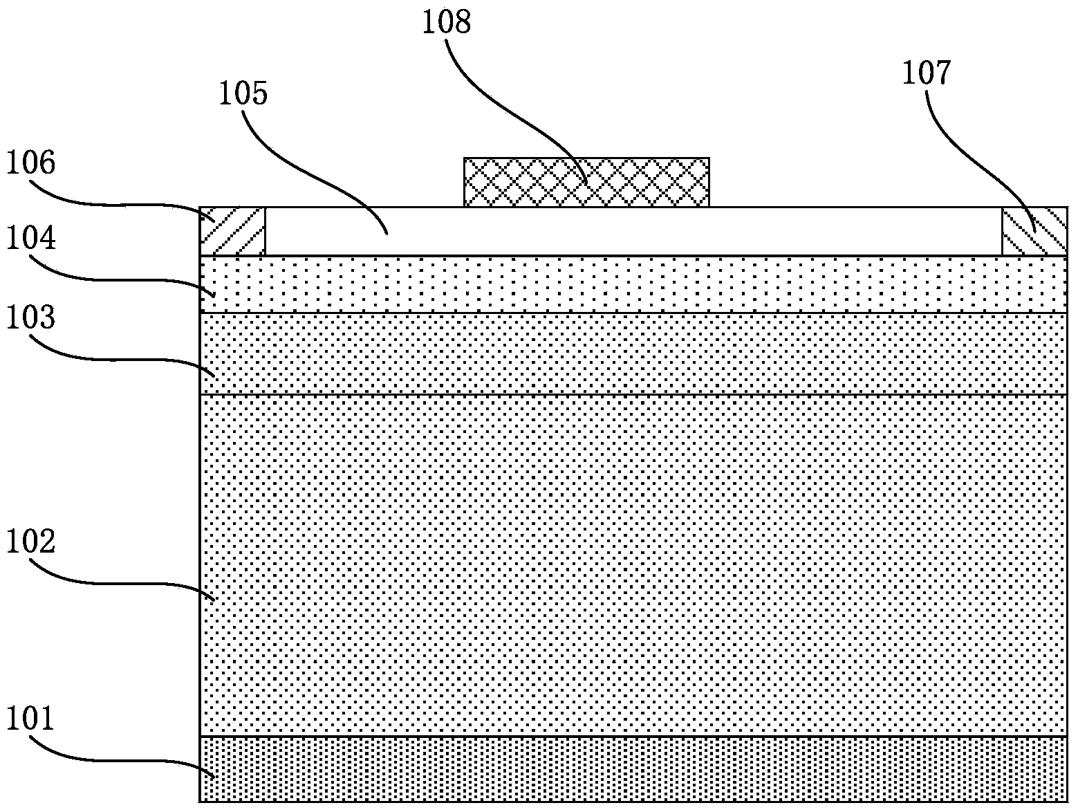
[0025] The easiest example to illustrate the purpose and advantages of the present invention to improve the frequency characteristics is provided by the present invention figure 2 The GaN MIS-HFET with the composite gate dielectric layer and the conventional structure GaN MIS-HFET ( figure 1 ) performance comparison; the structural parameters of the specific examples of the above two devices are given in Table 1.

[0026] Table 1 Microwave device simulation structure parameters

[0027]

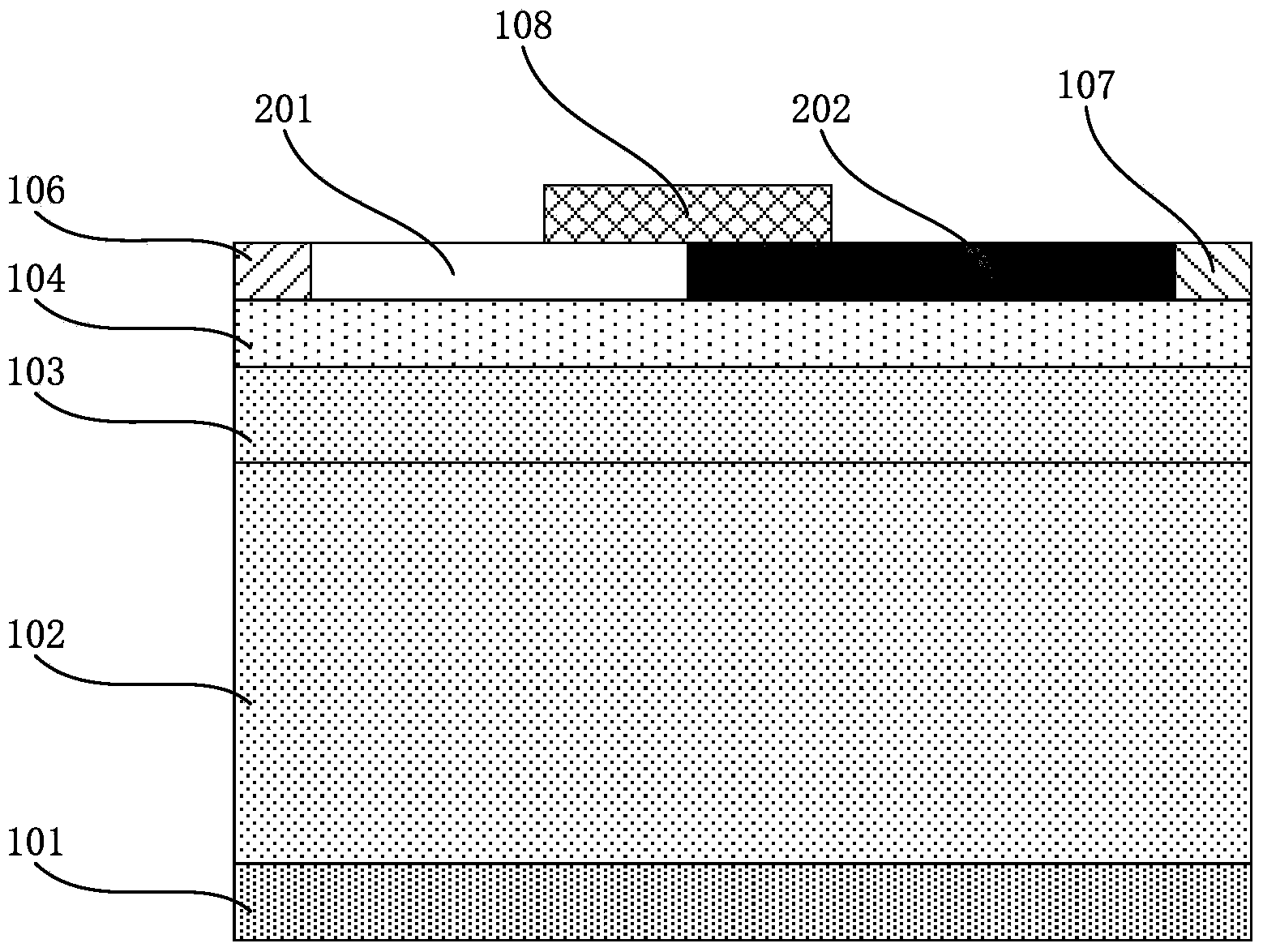
[0028] Provided based on the present invention such as image 3 In the GaN HEMT structure shown, the main process steps of the GaN HEMT provided in this embodiment are as follows: First, a gallium nitride buffer layer 102, a gallium nitride channel layer 103, and an aluminum gallium nitride layer are sequentially grown on a substrate 101 by MOCVD. (AlGaN) barrier layer 104, and then grow high dielectric constant dielectric layer 201 and low dielectric constant dielectric layer 202 respe...


PUM


Abstract

The invention discloses a gallium-nitride-based heterojunction field effect transistor with a combined gate dielectric layer. The gallium-nitride-based heterojunction field effect transistor sequentially and mainly comprises a substrate, a gallium nitride buffering layer, a gallium nitride channel layer, an aluminum gallium nitrogen barrier layer and the combined gate dielectric layer from bottom to top. A source, a drain and a gate are formed on the barrier layer, wherein the source and the drain are in ohmic contact with the barrier layer, and the gate is in schottky contact with the barrier layer. The combined gate dielectric layer is composed of gate dielectric layer bodies different in dielectric constant. In this way, an electric field peak value is formed on the gate dielectric layer interface of the channel layer, a peak value of the electron drifting speed exists at the portion of the electric field peak value, and the drifting speed of electrons in a whole channel is accordingly increased; meanwhile, due to the gate dielectric layer body with the low dielectric constant, the gate capacitance is reduced, and the frequency characteristic of a device is improved.

Description

technical field [0001] The invention relates to the field of semiconductor devices, in particular to a gallium nitride-based heterojunction field effect transistor with a composite gate dielectric layer. Background technique [0002] Gallium nitride (GaN) based heterojunction field effect transistor has excellent characteristics such as large band gap, high critical breakdown electric field, high electron saturation velocity, good thermal conductivity, radiation resistance and good chemical stability. (GaN) materials can form two-dimensional electron gas heterojunction channels with high concentration and high mobility with materials such as aluminum gallium nitride (AlGaN), so they are especially suitable for high-voltage, high-power and high-temperature applications, and are the most suitable for power electronics applications. One of the most promising transistors. [0003] figure 1 It is a schematic diagram of a traditional GaN MIS-HFET structure based on the prior art...

Claims


Application Information

Patent Timeline
IPC IPC(8): H01L29/78H01L29/43H01L29/10
CPCH01L29/511H01L29/66477H01L29/78
Inventor 杜江锋潘沛霖王康刘东于奇
Owner UNIV OF ELECTRONIC SCI & TECH OF CHINA
Why Eureka
Try Eureka