A three-dimensional cross-scale carbon electrode array structure and its preparation method
An array structure, cross-scale technology, applied in the field of three-dimensional cross-scale carbon electrode array structure and its preparation, can solve the problems of long preparation time, and achieve the effect of simple preparation method, good repeatability and large specific surface area
- Summary
- Abstract
- Description
- Claims
- Application Information
AI Technical Summary
Problems solved by technology
Method used
Image
Examples
preparation example Construction
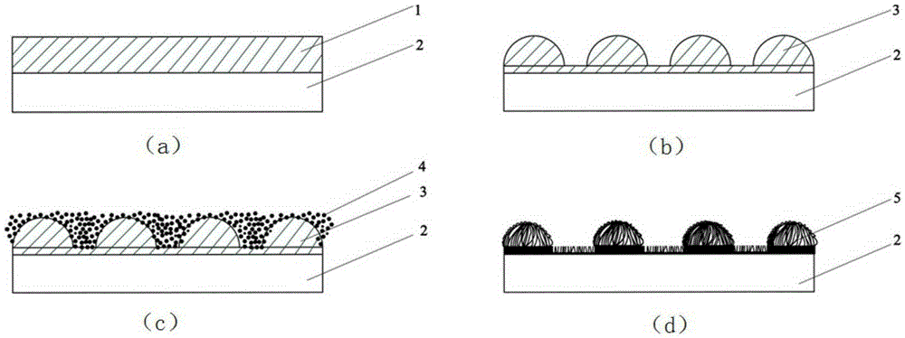
[0028] The preparation method of the three-dimensional cross-scale carbon electrode array structure of the present invention comprises the following steps:
[0029] (1) Pretreatment: Clean the silicon wafer to remove surface impurities and oxide layers.
[0030] (2) Coating a negative photoresist on the pretreated silicon wafer and performing pre-baking. The reason for choosing the negative resist as the precursor is that the negative resist can become a carbon structure when pyrolyzed in an inert gas, while the positive resist will volatilize when pyrolyzed at high temperature.
[0031] (3) Using a polydimethylsiloxane (polydimethylsiloxane, PDMS) template as an imprint template to perform an imprint process to obtain a photoresist hemispherical array structure.
[0032] Specifically, the imprinting temperature is 95° C., the pressure is 10 MPa, and the exposure time is 60 s.
[0033] (4) Etching with oxygen plasma to obtain a cross-scale photoresist array structure.
[00...
Embodiment 1
[0048] The preparation method of the three-dimensional cross-scale carbon electrode array structure of the embodiment of the present invention includes the following steps:
[0049] (1) Pretreatment: Clean the silicon wafer to remove surface impurities and oxide layers. Specifically, first place the silicon wafer in acetone for 10 minutes and then rinse it with deionized water; then put the silicon wafer into an SPM solution (a mixture of concentrated sulfuric acid and hydrogen peroxide at a volume ratio of 2:1) and heat it to 150°C After keeping for 10 minutes, rinse it with a large amount of deionized water; finally place the silicon wafer on a hot plate (Stuart, SD160) at 130°C for 30 minutes, then remove it and cool it to room temperature.
[0050] (2) Coat the pretreated silicon wafers (SU-8GM1070, KW-4A colloid machine). Specifically, first rotate at 500rpm for 10s, then at 1000rpm for 30s; then pre-bake on a hot plate, first keep at 65°C for 15min, then at 95°C for 30m...
Embodiment 2
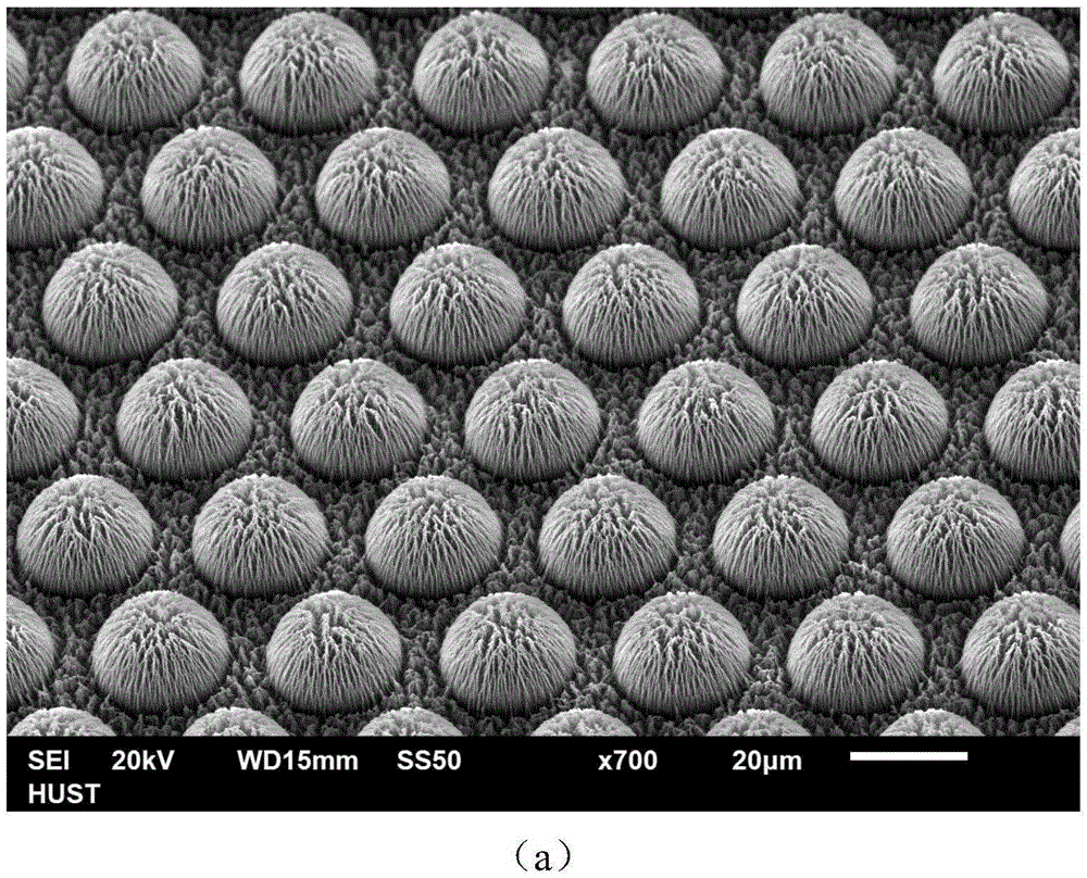
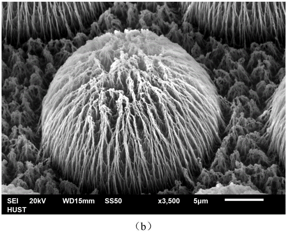
[0073] The oxygen plasma treatment time of step (4) in Example 1 was changed to 5 minutes, and other steps were the same as in Example 1. The cross-scale SU-8 array structure is obtained as Figure 4 (a) and Figure 4 (b) shown. Due to shortening the treatment time of oxygen plasma, the removed part of the obtained micro-nano structure is reduced, and a lot of photoresist in the center of the hemisphere has not been removed, and the formed structure has micro-nano structure on the surface, while the inner part The structure is again a solid photoresist structure.
PUM
 Abstract
Description
Claims
Application Information
 - R&D
- Intellectual Property
- Life Sciences
- Materials
- Tech Scout
- Unparalleled Data Quality
- Higher Quality Content
- 60% Fewer Hallucinations
Browse by: Latest US Patents, China's latest patents, Technical Efficacy Thesaurus, Application Domain, Technology Topic, Popular Technical Reports.
© 2025 PatSnap. All rights reserved.Legal|Privacy policy|Modern Slavery Act Transparency Statement|Sitemap|About US| Contact US: help@patsnap.com


