Method for preparing noncrystalline-nanocrystalline composite membrane by adopting co-sputtering method
A nanocrystalline composite and co-sputtering technology, which is applied in the preparation of mixture metal thin films, and in the field of preparation of amorphous-nanocrystalline composite films by co-sputtering, can solve problems that have not yet been discovered and achieve high creep strain rate sensitivity Exponential, strong operability, uniform plastic deformation effect
- Summary
- Abstract
- Description
- Claims
- Application Information
AI Technical Summary
Problems solved by technology
Method used
Image
Examples
Embodiment 1
[0040] 1) Ultrasonic the single-sided polished single crystal silicon substrate with acetone and alcohol for 15 minutes respectively, blow dry, put it on the rotatable substrate support frame of the vacuum magnetron sputtering equipment, and prepare for coating;
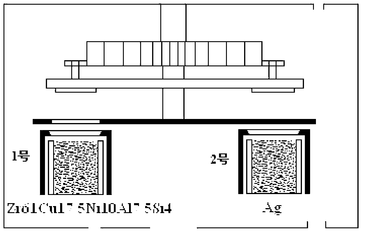
[0041] 2) will be represented by Zr 61 Cu 17.5 Ni 10 Al 7.5 Si 4 As the source target for obtaining the amorphous phase, it is placed on the No. 1 target base as the No. 1 target, and the Ag metal source target is placed on the No. 2 target base as the No. 2 target. The purity of the sputtering target is uniform. 99.99%. When working, first rotate the substrate to the middle above the No. 1 target and No. 2 target, and then pump the air pressure of the vacuum chamber to 3×10 -7 Pa, pass 3 sccm of Ar gas into the vacuum chamber, and change the sputtering power by adjusting the current and voltage to control the proportion of amorphous and nanocrystalline components, and adjust the residence time of the substrate ...
Embodiment 2
[0043] This embodiment adopts Zr 61 Al 7.5 Cu 17.5 Ni 10 Si 4 (at%) is used as the source target material to obtain the amorphous phase, and metal Ag is used as the metal source target material to obtain the nanophase, and a mixture material in which the amorphous phase and the nanocrystalline phase coexist uniformly is prepared.
[0044] The specific process of ZrCuNiAlSi amorphous / nanocrystalline Ag co-sputtering thin film material:
[0045] 1) Cut the single-sided polished single-crystal silicon wafer into the required size with a diamond blade, then ultrasonically clean it with acetone and absolute alcohol for 20 minutes, dry it with a hair dryer, and put it into an ultra-high vacuum magnetron sputtering equipment on a rotatable base support.
[0046] 2) if figure 1 shown, according to Zr 61 Al 7.5 Cu 17.5 Ni 10 Si 4 (at%) Atomic percentage, the five-element alloy target obtained by pressing the pure element powder with a purity of more than 99.99% is placed on...
Embodiment 3
[0054] The specific process parameters of the amorphous-W co-sputtering film preparation method in this embodiment are as follows: adjust the DC magnetron sputtering power of the W target to 25w, the DC magnetron sputtering voltage of the W target during co-deposition is 375V, and the Ar gas flow rate is 3 sccm, a bias voltage of 100V, and a substrate temperature of room temperature, thereby obtaining an amorphous-W co-sputtered film in which the nanocrystalline W phase and the amorphous phase coexist uniformly.
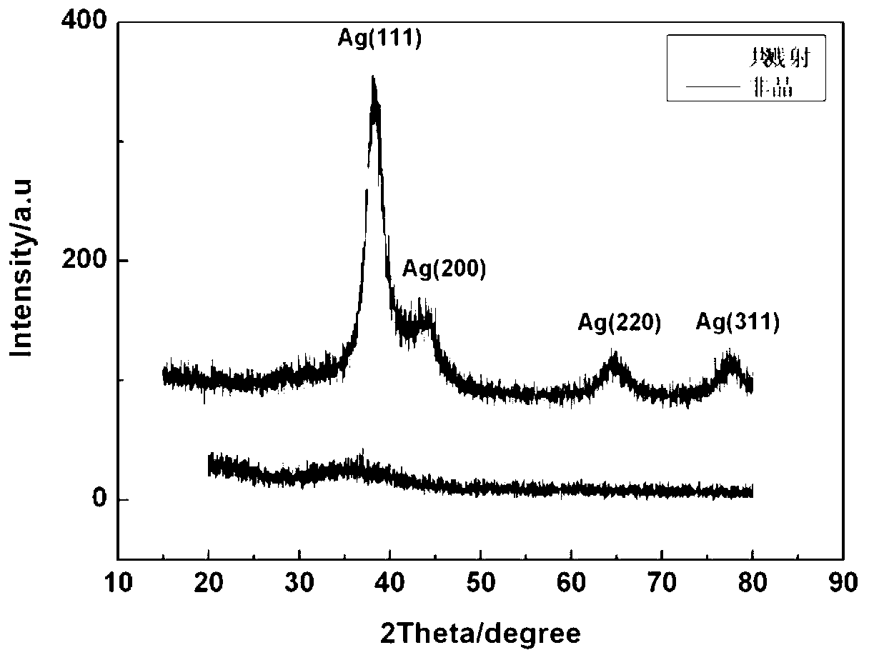
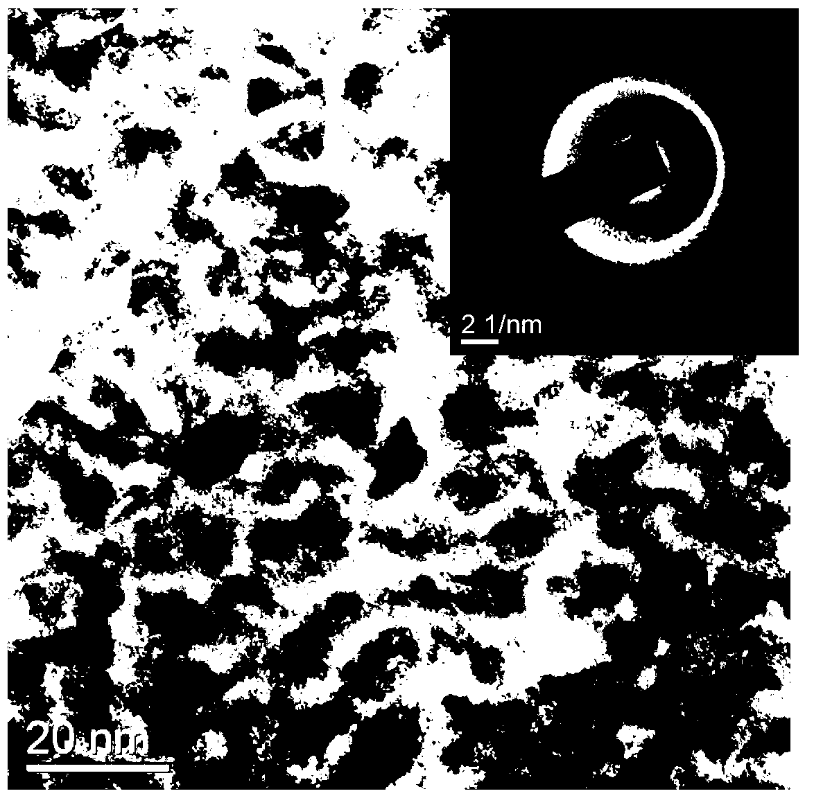
[0055] Figure 6 for Zr 61 Al 7.5 Cu 17.5 Ni 10 Si 4 From the XRD analysis of the amorphous thin film and the amorphous-W co-sputtered film, it can be seen that the diffraction peaks of the amorphous-W co-sputtered film are sharper, indicating that the sample has a tendency to crystallize, but due to this diffraction The peak is very broad and needs to be further confirmed by high-resolution transmission (HRTEM) observation.
[0056] Figure 7 It is the TEM im...
PUM
| Property | Measurement | Unit |
|---|---|---|
| purity | aaaaa | aaaaa |
Abstract
Description
Claims
Application Information
 - R&D
- Intellectual Property
- Life Sciences
- Materials
- Tech Scout
- Unparalleled Data Quality
- Higher Quality Content
- 60% Fewer Hallucinations
Browse by: Latest US Patents, China's latest patents, Technical Efficacy Thesaurus, Application Domain, Technology Topic, Popular Technical Reports.
© 2025 PatSnap. All rights reserved.Legal|Privacy policy|Modern Slavery Act Transparency Statement|Sitemap|About US| Contact US: help@patsnap.com


