
Metal gate field effect transistor and manufacturing method thereof

A technology for field effect transistors and metal gates, which is applied in the field of metal gate field effect transistors and its production, can solve the problems of increasing the aspect ratio and increasing the difficulty of filling metal, so as to reduce parasitic resistance and save process costs , The effect of improving process efficiency

Active Publication Date: 2013-07-03
SEMICON MFG INT (SHANGHAI) CORP
View PDF6 Cites 3 Cited by
  • Summary
  • Abstract
  • Description
  • Claims
  • Application Information

AI Technical Summary

Problems solved by technology

[0007] And with the development of integrated circuit technology to the deep sub-micron level, smaller and smaller transistors make the contact holes / vias in the metal interconnection structure in integrated circuits face the problem of increasing their aspect ratio, so in the follow-up During the metallization process, it is more difficult to fill the metal in the via hole with high aspect ratio. The existing filling method of metal sputtering makes it inevitable that there will be voids or voids in the metal in the formed via hole. crack

Method used


Image

  • Metal gate field effect transistor and manufacturing method thereof
  • Metal gate field effect transistor and manufacturing method thereof
  • Metal gate field effect transistor and manufacturing method thereof

Examples


Embodiment Construction

[0027] The present invention provides a method for manufacturing a metal gate field effect transistor, which uses a gate-last process to fabricate a dummy gate, and then forms at least a part of the metal gate stack and the source and drain by electrodeless electroplating (Electroless deposition, electroless plating) contact holes. In the present invention, the last layer of the metal gate and the contact holes of the source and drain electrodes are formed by means of electroless metal plating, so that the trenches and contact holes formed by the metal in the metal gate are used in through holes with high aspect ratios. The metal texture is dense and uniform, and there are no voids and cracks; and the present invention forms the last layer of metal of the metal gate together with the contact hole, which saves process steps, improves process efficiency and saves process cost; at the same time, the present invention The parasitic resistance Rcsd of the contact hole and the drain...


PUM


Abstract

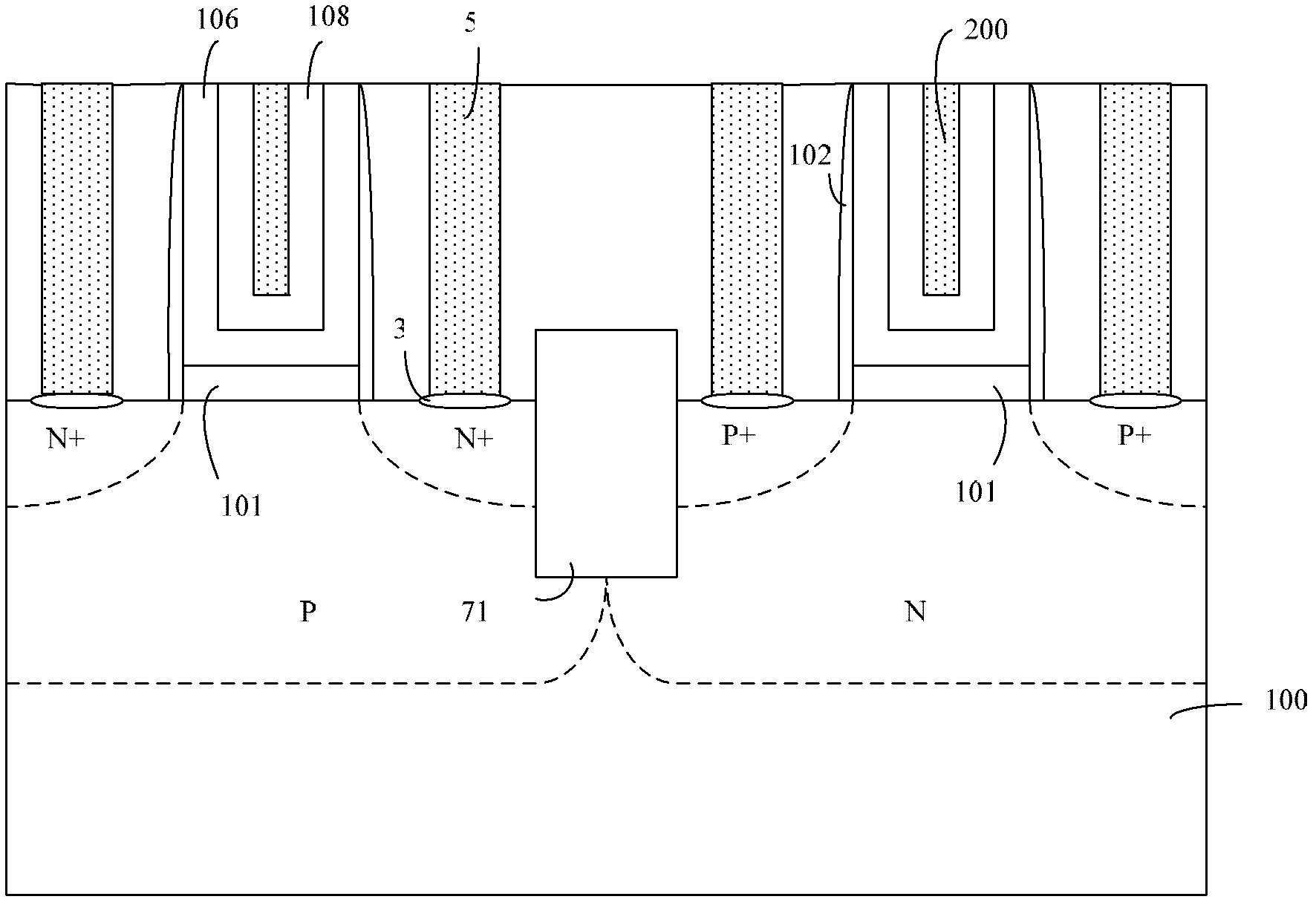
Provided is a metal gate field effect transistor and a manufacturing method thereof. The manufacturing method of the metal gate field effect transistor comprises the following steps: forming dummy gates by applying a gate-last approach; removing the dummy gates to form openings; sequentially forming work function metal material layers and metal barrier layers on the lateral walls and the bottoms of the openings, wherein the work function metal material layers and the metal barrier layers are not fully filled with the openings; forming through holes of contact holes above a source electrode and a drain electrode; and forming filler metal layers in an electrodeless electroplating mode, wherein the filler metal layers are filled with the openings and the through holes in the contact holes. By utilizing the electrodeless electroplating metal mode to form a last layer of metal gates and the contact holes of a source region and a drain region, metal texture of metal in the metal gates and the through holes of which a high aspect ratio is same as the contact holes is compact and even, and is free of cavities and gaps. Process steps are saved, process efficiency is improved, and process cost is saved. In the meanwhile, by selecting the metal filled in the contact holes, the metal gate field effect transistor and the manufacturing method thereof can reduce parasitic resistance of the contact holes and the drain electrode.

Description

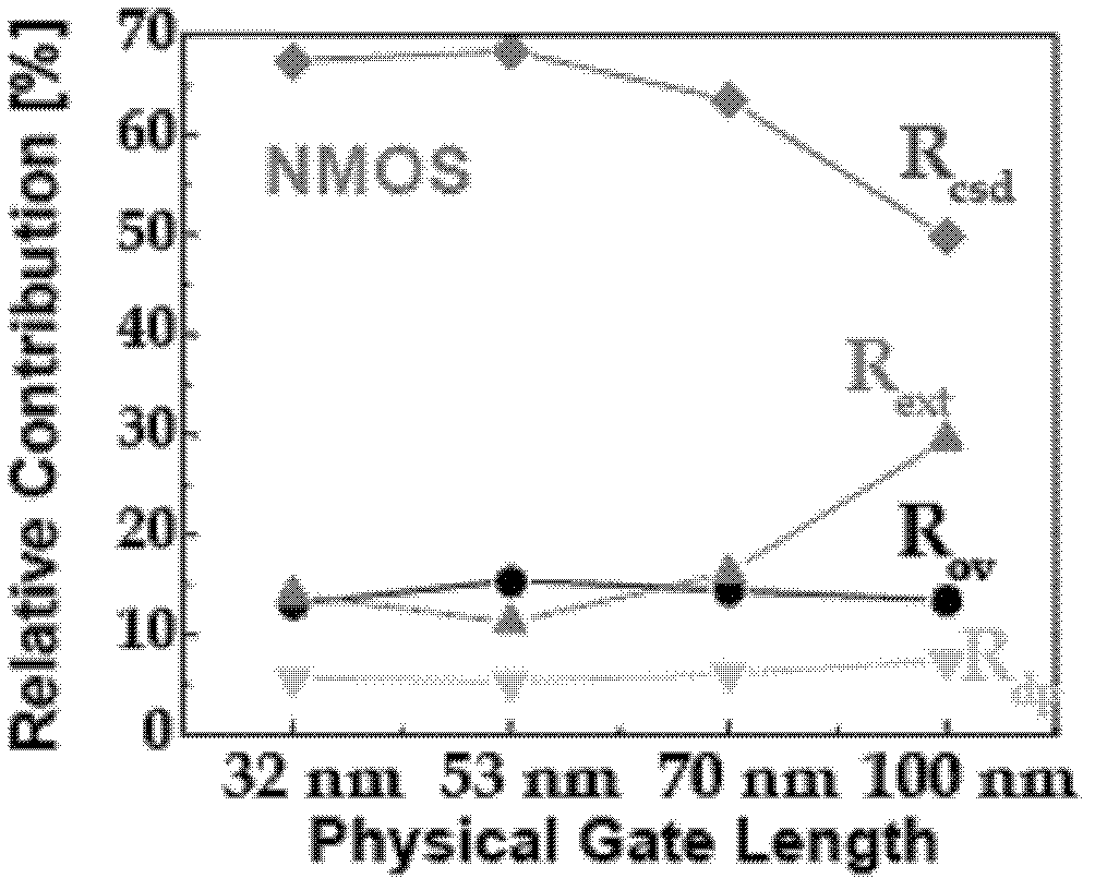
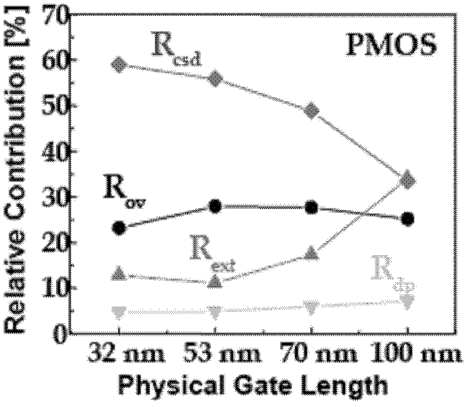
technical field [0001] The invention relates to the field of semiconductor manufacturing, in particular to a metal gate field effect transistor and a manufacturing method thereof. Background technique [0002] In the actual MOSFET, its equivalent circuit includes the parasitic series resistance of the source and drain. Each resistance is composed of three parts: the contact resistance between the metal and the source and drain regions; the bulk resistance of the source and drain regions; related resistance. Figure 1 to Figure 2 The figure shows the parasitic resistance of NMOS and PMOS in the technology node where the critical dimension of the integrated circuit develops from 100nm to 32nm. It can be seen that Rcsd (the contact resistance between the metal and the source and drain regions) accounts for an increasing proportion of the entire parasitic resistance, and its value is also increasing. So it is necessary to reduce Rcsd in today's state-of-the-art technology. ...

Claims


Application Information

Patent Timeline
Patent Type & Authority Applications(China)
IPC IPC(8): H01L21/336H01L21/28H01L29/78H01L29/423
Inventor 平延磊
Owner SEMICON MFG INT (SHANGHAI) CORP
Learn More