The Method of Improving the Resistance Value Accuracy of Buried Resistor Printed Circuit Board

A technology for printed circuit boards and embedded resistors, which is applied in the direction of containing printed electrical components and removing conductive materials by chemical/electrolytic methods, which can solve the problems of inability to make small-sized resistors, poor precision, and poor stability, and achieve realization The effects of mass production, reduced processing difficulty, and improved resistance value accuracy

Active Publication Date: 2015-08-26
DONGGUAN SHENGYI ELECTRONICS
View PDF5 Cites 0 Cited by
  • Summary
  • Abstract
  • Description
  • Claims
  • Application Information

AI Technical Summary

Problems solved by technology

[0003] Buried resistor printed circuit boards often use buried resistor ink (Asahi's TU-XX-08 series) as buried resistors for processing. Due to the limitations of silk screen printing technology and equipment, small-sized resistors cannot be made, and the resistor line width must be greater than 15mil; at the same time Screen printing production is extremely difficult, with poor precision, poor reproducibility, and poor stability. Under the current production conditions, the promotion of this process is slow, and most of them are in the stage of prototype and small batch production.

Method used


Image

  • The Method of Improving the Resistance Value Accuracy of Buried Resistor Printed Circuit Board
  • The Method of Improving the Resistance Value Accuracy of Buried Resistor Printed Circuit Board
  • The Method of Improving the Resistance Value Accuracy of Buried Resistor Printed Circuit Board

Examples


Embodiment Construction

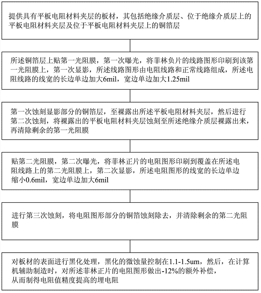
[0031] In order to further illustrate the technical means adopted by the present invention and its effects, the following describes in detail in conjunction with preferred embodiments of the present invention and accompanying drawings.

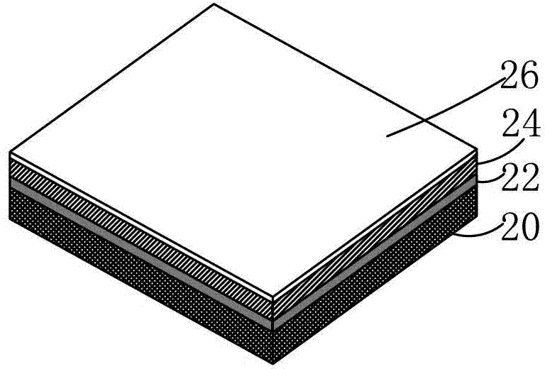
[0032] see Figure 1-Figure 4 , the present invention provides a kind of method that improves the resistance value precision of buried resistor printed circuit board, and its technological process is as follows:

[0033] The first development → water washing → the first etching (etching copper, acid etching DES) → water washing → the second etching (etching Ohmega-ply material, acid etching) → water washing → film removal → the second development → water washing → the second Three times of etching (copper etching, alkali etching SES)→water washing→second film removal.

[0034] The technical process of the buried resistance printed circuit board of the present invention is as follows:

[0035] Cutting material → pasting the first photoresist ...


PUM


Abstract

The invention provides a method for improving the accuracy of a resistance value of a buried resistance printed circuit board. The method comprises the following steps of: 1, providing a board with a buried resistance layer, wherein the board comprises an insulating dielectric layer, the buried resistance layer and a copper foil layer; 2, pasting a first photoresist film, performing primary exposure, printing a line graph of a negative film on the first photoresist film, and performing primary development, wherein the line graph consists of a resistance line and a normal line, each of long sides of a line width of the resistance line is prolonged by 6mil, and each of wide sides of the line width of the resistance line is prolonged by 1.25mil; 3, performing primary etching and secondary etching; 4, pasting a second photoresist film, performing secondary exposure, printing a resistance graph of a positive film on the second photoresist film, and performing secondary development, wherein each of long sides of a line width of the resistance graph is shortened by 0.6mil, and each of wide sides of the line width of the resistance graph is widened by 6mil; 5, performing tertiary etching; and 6, performing blackening treatment on the surface of the board in a way of controlling a microetching amount within 1.1 to 1.5 mu.m, and performing additional compensation of -12 percent on the resistance graph of the positive film.

Description

technical field [0001] The invention relates to a buried element type printed circuit board, in particular to a method for improving the resistance value precision of a buried resistor printed circuit board. Background technique [0002] In order to improve the assembly density and performance of products and reduce the volume and weight of products, it is an effective way to integrate passive components into circuit boards, so printed circuit boards with buried resistors emerge as the times require. Buried resistance printed circuit boards have the following advantages in the design of high-speed transmission circuits: improve the impedance matching of the line, shorten the path of signal transmission, reduce parasitic inductance, eliminate the inductance generated in the surface mount or plug-in process, and reduce signal crosstalk , noise and electromagnetic interference. [0003] Buried resistance printed circuit boards often use buried resistance ink (TU-XX-08 series o...

Claims


Application Information

Patent Timeline
Patent Type & Authority Patents(China)
IPC IPC(8): H05K3/06H05K1/16
Inventor 杜红兵焦其正李民善曾红
Owner DONGGUAN SHENGYI ELECTRONICS
Why Eureka
Try Eureka