Method of producing printed circuit board incorporating resistance element

A technology for printed wiring boards and manufacturing methods, which can be used in the fields of printed circuit manufacturing, electrical components, multilayer circuit manufacturing, etc., and can solve problems such as inability to respond to resistance changes, difficulties, etc.

Inactive Publication Date: 2008-12-10
NIPPON MEKTRON LTD
View PDF4 Cites 0 Cited by
  • Summary
  • Abstract
  • Description
  • Claims
  • Application Information

AI Technical Summary

Problems solved by technology

[0022] The terminating resistors of transmission lines and the resistors used in EMI filters are required to have an accuracy of ±1% or less. However, according to the current technology, in the built-in resistor element formed of resistor paste, it cannot be compared with the resistor before and after lamination. Due to variations, it is difficult to achieve an accuracy of ±1% or less with a good yield depending on the built-in state

Method used


Image

  • Method of producing printed circuit board incorporating resistance element
  • Method of producing printed circuit board incorporating resistance element
  • Method of producing printed circuit board incorporating resistance element

Examples


Embodiment 1

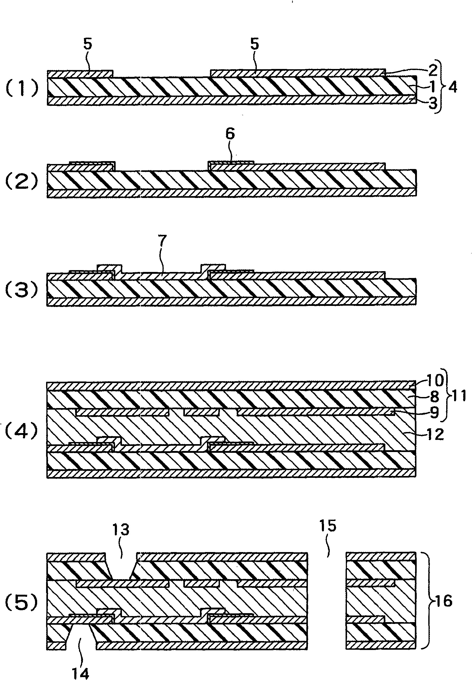
[0051] Figure 1A , Figure 1B It is a cross-sectional process view showing the manufacturing steps of the printed wiring board with built-in resistor element according to one embodiment of the present invention. First, if Figure 1A As shown in (1), a so-called double-sided copper-clad laminate 4 having a first metal foil 2 such as copper foil and a second metal foil 3 on both sides of an insulating base material 1 such as polyimide is prepared. Then, at a desired position of the first metal foil 2, a circuit is formed at the same time as the electrode 5 of the resistive paste is formed using an etching method by a usual photoprocessing method.

[0052]In addition, 25 μm thick polyimide was used as the base material, and 12 μm electrolytic copper foil was used as the metal foil. The resistance value is determined by the width and film thickness of the resistance paste, the distance between electrodes, and the sheet resistance value of the paste, and here, the distance betwee...

Embodiment 2

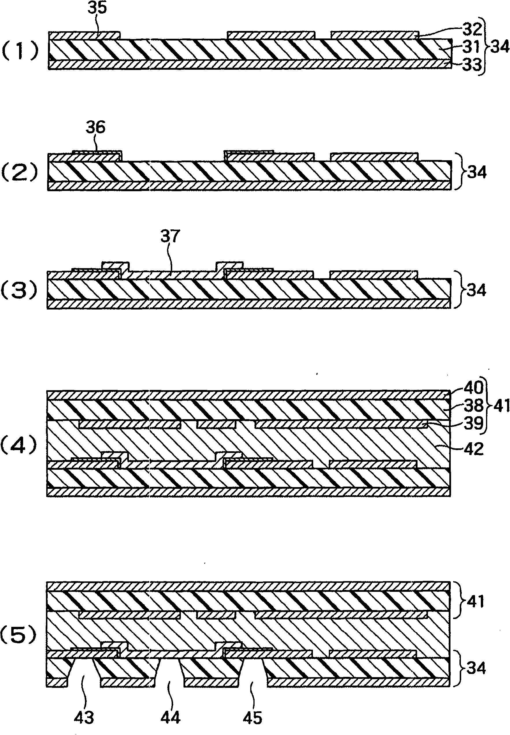
[0067] Figure 2A , Figure 2B It is a cross-sectional step diagram showing a method of manufacturing a printed wiring board with a built-in resistance element in one embodiment of the present invention. First, as Figure 2A As shown in (1), a so-called double-sided copper-clad laminate 34 having a first metal foil 32 such as copper foil and a second metal foil 33 on both sides of an insulating base material 31 such as polyimide is prepared. Desired positions of the foil 32 are etched using a common photoprocessing method, and a circuit is formed simultaneously with the electrodes 35 of the resistor paste.

[0068] In addition, 25 μm thick polyimide was used as the base material, and 12 μm electrolytic copper foil was used as the metal foil. The resistance value is determined by the width and film thickness of the resistance paste, the distance between electrodes, and the sheet resistance value of the paste, and here, the distance between electrodes is set to 1.0 mm.

[006...


PUM

PropertyMeasurementUnit
thicknessaaaaaaaaaa

Abstract

The present invention provides a method of producing a resistance element incorporated in a printed circuit board at an accuracy of resistance value of +-1% or less, at low cost and with a good yield while the resistance element formed by a resistor paste is incorporated. A method of producing a printed circuit board incorporating a resistance element includes: preparing a double-sided copper clad board having a first metallic foil on one face of an insulating base material thereof and a second metallic foil on the other face of the insulating base material thereof; providing at least a pair of electrodes on one of the metallic foils; printing a resistor paste between the electrodes to form a resistor; preparing a circuit board having at least one wiring layer; ; causing a layer on which the resistor paste is formed to oppose the circuit board to layer the double-sided copper clad board on the circuit board; forming openings in the first and the second metallic foils; and emitting laser through the openings to partly remove the insulating base material and the resistor paste to adjust resistance value. A conformal mask for etching may be formed on the second metallic foil to form openings in the insulating base material by etching to emit laser through the openings.

Description

technical field [0001] The present invention relates to a structure of a printed wiring board and a manufacturing method thereof, in particular to a printed wiring board with a built-in resistance element and a manufacturing method thereof. Background technique [0002] In recent years, along with the miniaturization and high performance of electronic equipment, the mounting density of components has increased significantly. Therefore, a component-embedded substrate is considered in which passive components such as resistors and capacitors are not soldered and mounted on the surface of a circuit substrate in the form of chip components as in the past, but passive components are formed on the inner surface of the substrate, thereby Improve installation density. [0003] In the method of forming resistors in passive components on the inner surface of the substrate, ceramic multilayer substrates have been used in practical use. However, since the resistors are formed by screen...

Claims


Application Information

Patent Timeline
Patent Type & Authority Applications(China)
IPC IPC(8): H05K1/16H05K3/46
CPCH05K1/167H05K3/0032H05K3/4611H05K2201/0187H05K2201/09509H05K2203/0554H05K2203/107H05K2203/1453H05K2203/171Y10T29/49082Y10T29/49099Y10T29/49126Y10T29/4913Y10T29/49155
Inventor 宫本雅郎
Owner NIPPON MEKTRON LTD
Why Eureka
Try Eureka