Floating resistance of I/O circuit on integrated circuit chip
A technology of integrated circuits and resistors, applied in the field of floating resistors of multiple I/O circuits, can solve problems such as increasing product cost, and achieve the effects of improving consistency, improving resistance value accuracy, and reducing external influences.
- Summary
- Abstract
- Description
- Claims
- Application Information
AI Technical Summary
Problems solved by technology
Method used
Image
Examples
Embodiment 1
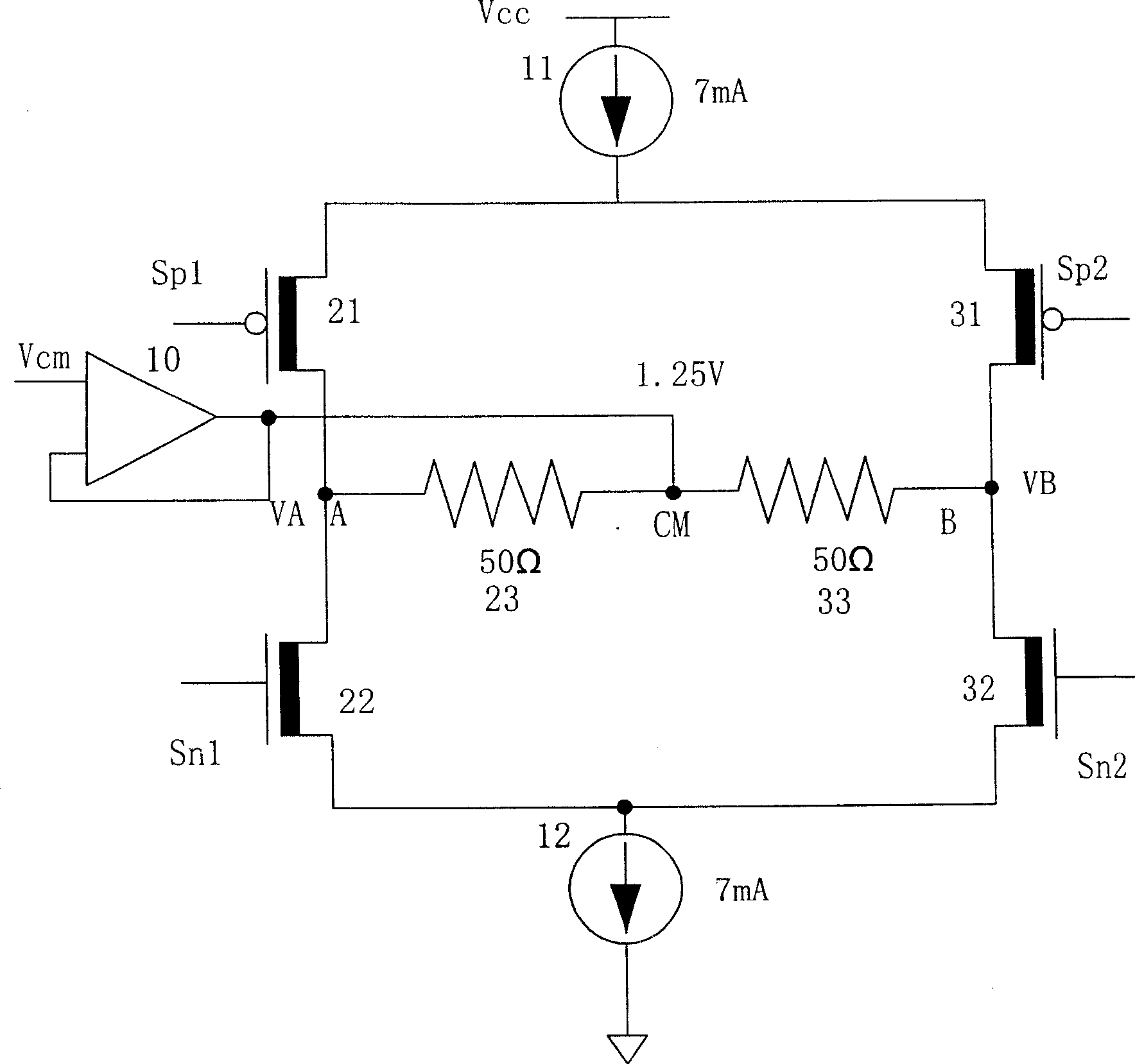
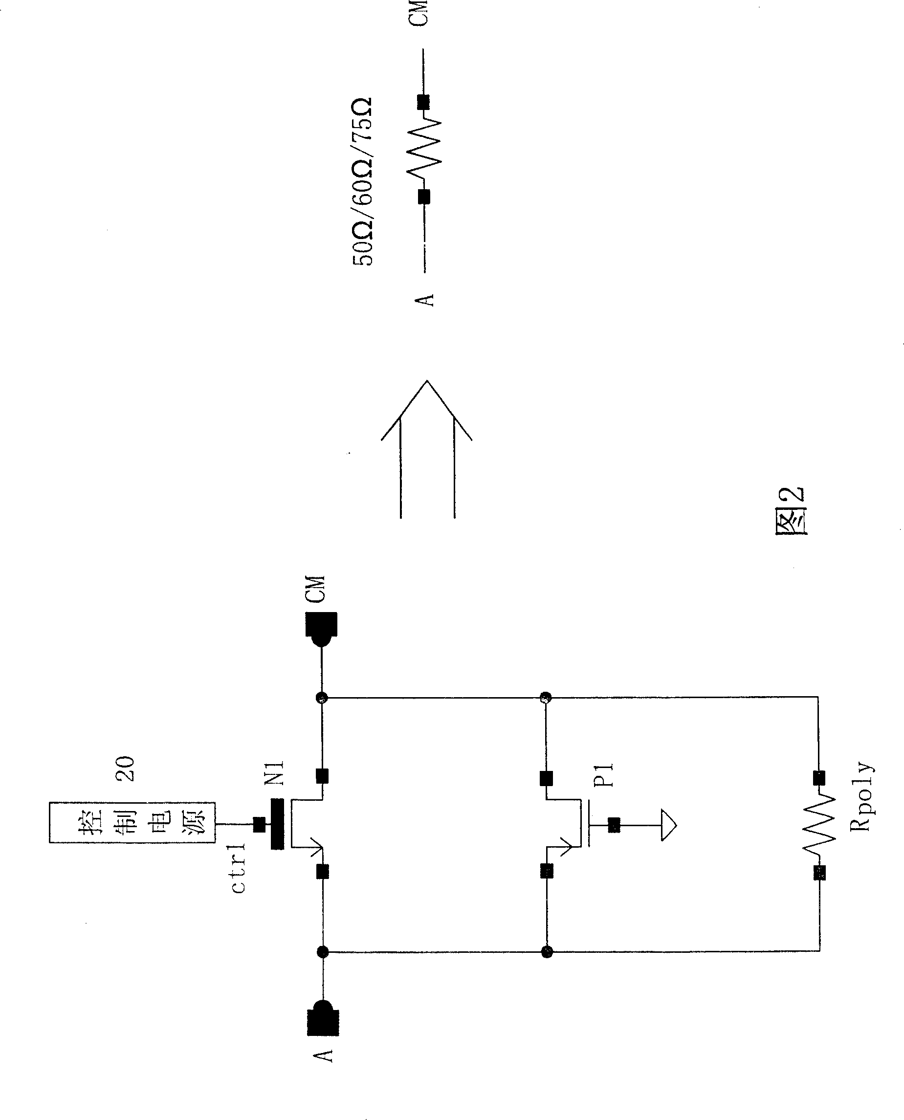
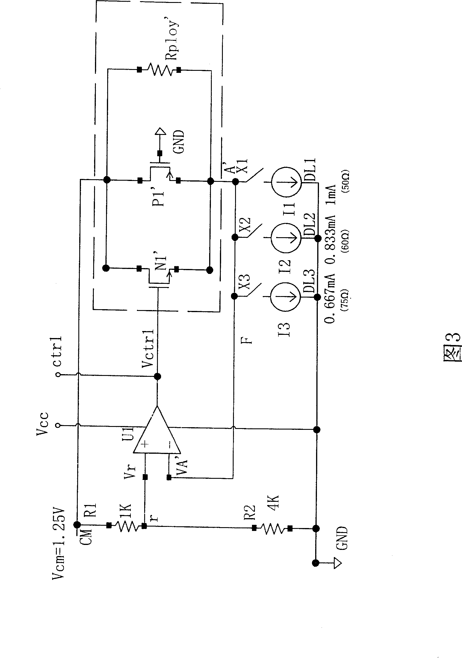
[0017] The electrical structure of a dual low-voltage differential signal I / O on a 17-channel dual low-voltage differential signal (LVDS) I / O integrated circuit chip, such as figure 1 Shown. A P-type FET 21 and an N-type FET 22 of the first group of low-voltage differential signal I / O are connected in series between the constant current source 11 connected to the power supply voltage Vcc and the constant current source 12 connected to the ground level , The grid Sp1 of the P-type FET 21 and the grid Sn1 of the N-type FET 22 are the two input terminals of the first group of low-voltage differential signals. A point A of the signal output terminal of the first group of low-voltage differential signal I / O, that is, the connection point of the P-type field effect transistor 21 and the N-type field effect transistor 22 is connected to a floating resistor 23. The other end of the floating resistor 23 is connected to the CM point and a constant voltage V is provided by an on-chip power ...
PUM
 Abstract
Description
Claims
Application Information
 - R&D
- Intellectual Property
- Life Sciences
- Materials
- Tech Scout
- Unparalleled Data Quality
- Higher Quality Content
- 60% Fewer Hallucinations
Browse by: Latest US Patents, China's latest patents, Technical Efficacy Thesaurus, Application Domain, Technology Topic, Popular Technical Reports.
© 2025 PatSnap. All rights reserved.Legal|Privacy policy|Modern Slavery Act Transparency Statement|Sitemap|About US| Contact US: help@patsnap.com


