Resistance wiring board and its mfg. method
A manufacturing method and wiring board technology, which is applied in the direction of resistance manufacturing, printed circuit manufacturing, resistors, etc., can solve the problems of height reduction, installation difficulty, thermal conductivity reduction of insulating substrate, etc., and achieve the effect of height reduction
- Summary
- Abstract
- Description
- Claims
- Application Information
AI Technical Summary
Problems solved by technology
Method used
Image

Examples
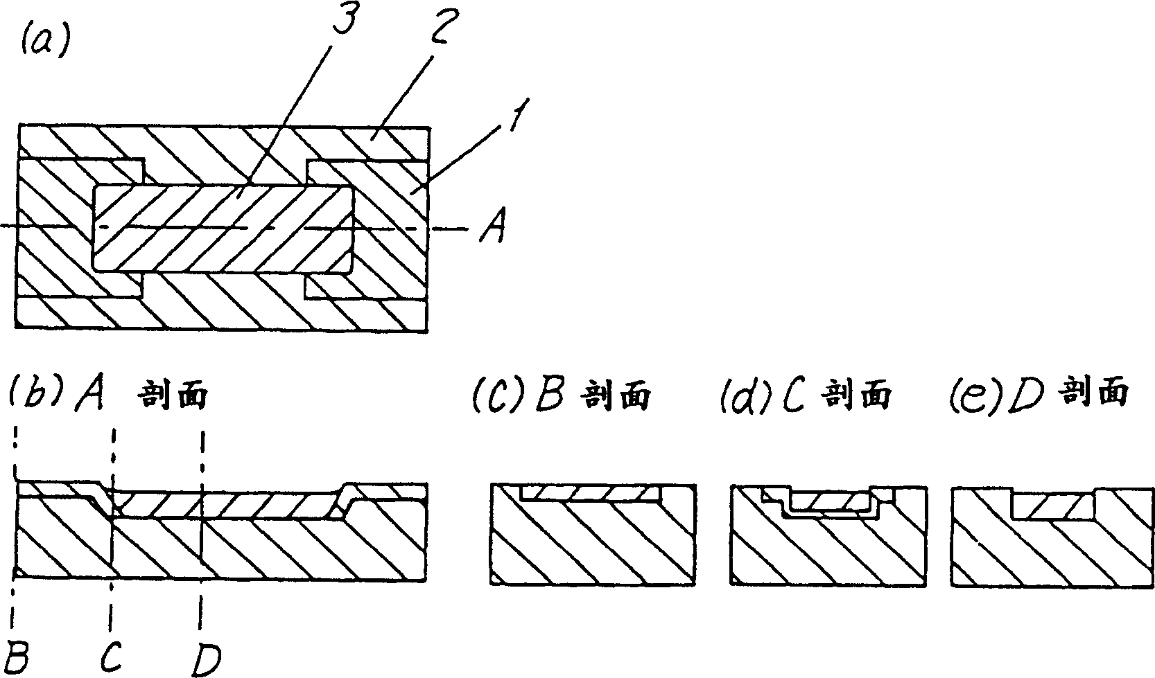
Embodiment 1
[0025] The resistance wiring board of Example 1 of the present invention can be obtained by a manufacturing method comprising the following steps: using a doctor blade method to mix and disperse aluminum powder and additives shown in Table 1, butyral resin, plasticizer, and solvent to obtain The paste, the first step of forming a green sheet, on the green sheet obtained by the first step, use the Pd-Ag paste of the composition shown in Table 1 and use the second step of screen printing to form an electrode pattern, and use the method to obtain a dense sintered substrate. The temperature of the sheet is the third step of sintering the green sheet obtained in the second step. After printing a ruthenium oxide series resistor paste as a resistor material between the electrodes on the sintered body obtained in the third step, print a resistive protective film. The fourth process of sintering the glass paste at 650°C.
[0026] Use Pd-Ag series or Pd electrodes containing more than 6...
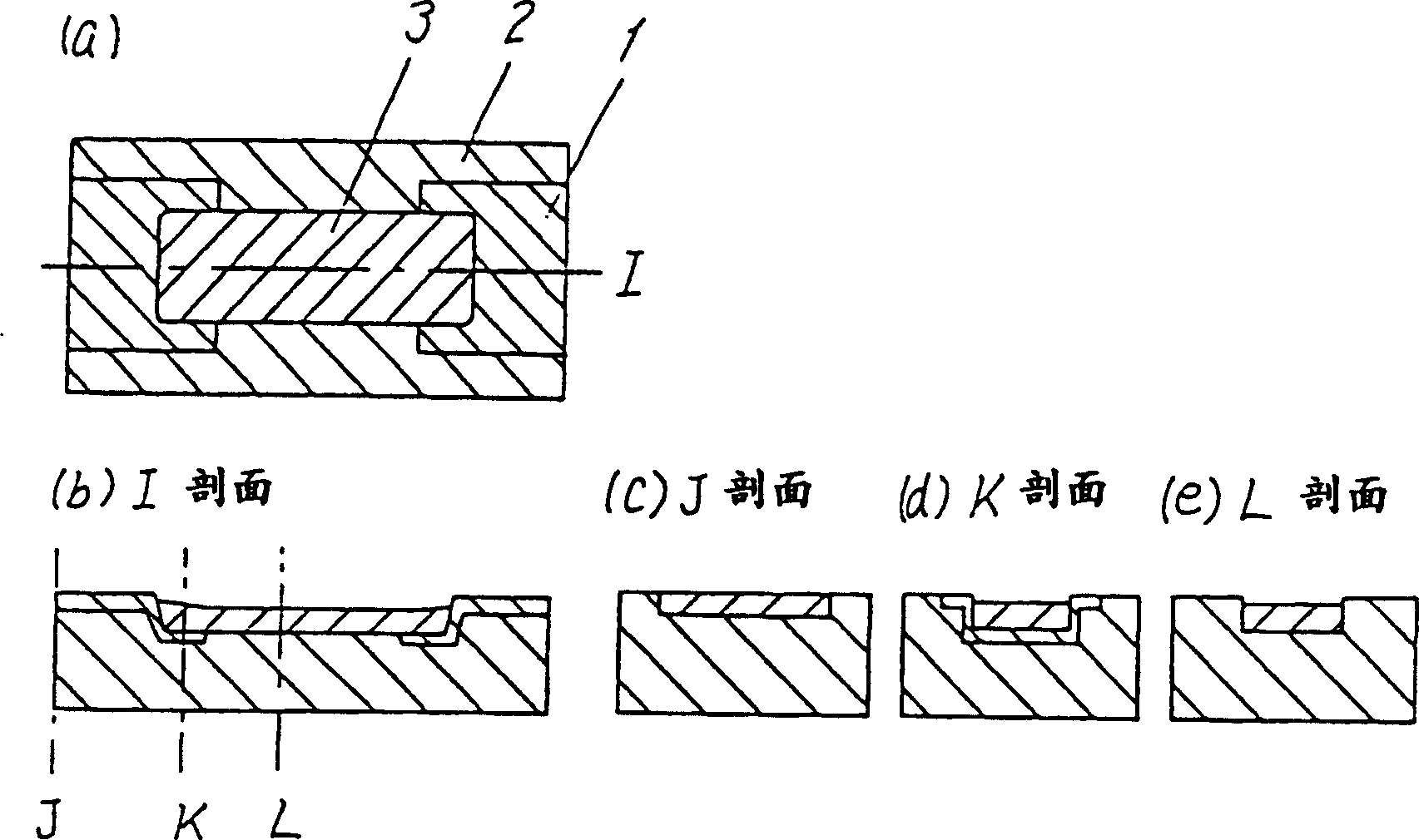
Embodiment 2
[0032] The resistance wiring board of Example 2 of the present invention can be obtained by a manufacturing method comprising the following steps: using a doctor blade method to mix aluminum: TiO2: MnO: SiO2 in a weight ratio of 94:2:2:2 Raw material powder and butylated The paste obtained by mixing and dispersing an aldehyde resin, a plasticizer, and a solvent to form a green sheet is the first step. On the green sheet obtained by the first step, a Pd paste is used to form an electrode pattern by screen printing. The second step is to The third step is to form a 40 μm-deep step between the electrode patterns on the green sheet obtained in the second step, and the fourth step is to sinter the molded body obtained in the third step at a temperature capable of obtaining a dense sintered substrate. In the step, the step on the sintered body obtained in the fourth step is filled with ruthenium oxide series resistor paste and glass paste, and then the fifth step is sintering at 650°...
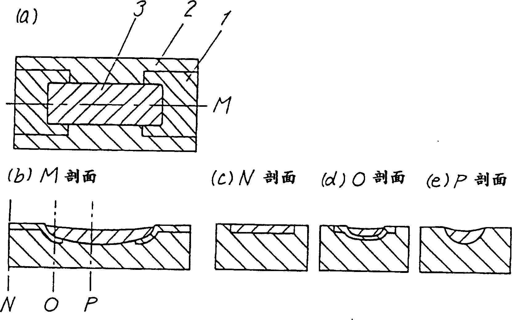
Embodiment 3
[0040] The resistance wiring board of Example 3 of the present invention can be obtained by a manufacturing method including the following steps: a paste obtained by mixing and dispersing raw material powder having the same composition as that of Example 2, a plasticizer, and a solvent by the doctor blade method , the first process of forming a green sheet, on the green sheet obtained by the first process, use Pd paste and use the second process of screen printing to form an electrode pattern, and form a step difference of 40 μm depth by the forming mold, so that the obtained in the second process The third step in which the electrode pattern on the green sheet overlaps the bottom surface of the step, the fourth step in which the molded body obtained in the third step is sintered at a temperature capable of obtaining a dense sintered substrate, and the sintered body obtained in the fourth step The fifth step of sintering is performed at 650°C after filling the ruthenium oxide s...
PUM
 Abstract
Description
Claims
Application Information
 - R&D
- Intellectual Property
- Life Sciences
- Materials
- Tech Scout
- Unparalleled Data Quality
- Higher Quality Content
- 60% Fewer Hallucinations
Browse by: Latest US Patents, China's latest patents, Technical Efficacy Thesaurus, Application Domain, Technology Topic, Popular Technical Reports.
© 2025 PatSnap. All rights reserved.Legal|Privacy policy|Modern Slavery Act Transparency Statement|Sitemap|About US| Contact US: help@patsnap.com