Method for removing silicon ridge produced in epitaxial deposition of super-junction high-pressure device

A high-voltage device and epitaxial deposition technology, which is applied in semiconductor/solid-state device manufacturing, electrical components, circuits, etc., can solve problems affecting and affecting the electrical properties of devices, and achieve the effect of avoiding impact and good surface morphology

Active Publication Date: 2013-03-27
SHANGHAI HUAHONG GRACE SEMICON MFG CORP
View PDF4 Cites 2 Cited by
  • Summary
  • Abstract
  • Description
  • Claims
  • Application Information

AI Technical Summary

Problems solved by technology

In the subsequent oxide film removal process, if the epitaxial layer filled in this part of the incision is not removed, silicon ridges will be formed on both sides of the trench, which will affect the subsequent process, thereby affecting some electrical properties of the device.

Method used


Image

  • Method for removing silicon ridge produced in epitaxial deposition of super-junction high-pressure device
  • Method for removing silicon ridge produced in epitaxial deposition of super-junction high-pressure device
  • Method for removing silicon ridge produced in epitaxial deposition of super-junction high-pressure device

Examples


Embodiment Construction

[0029] The present invention will be described in further detail below in conjunction with the accompanying drawings and embodiments.

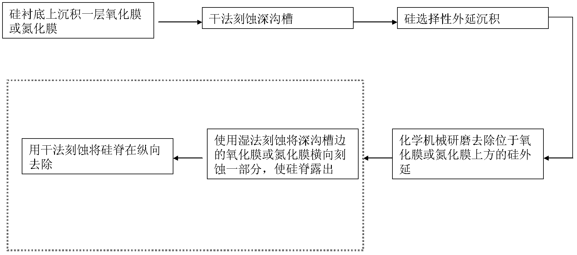
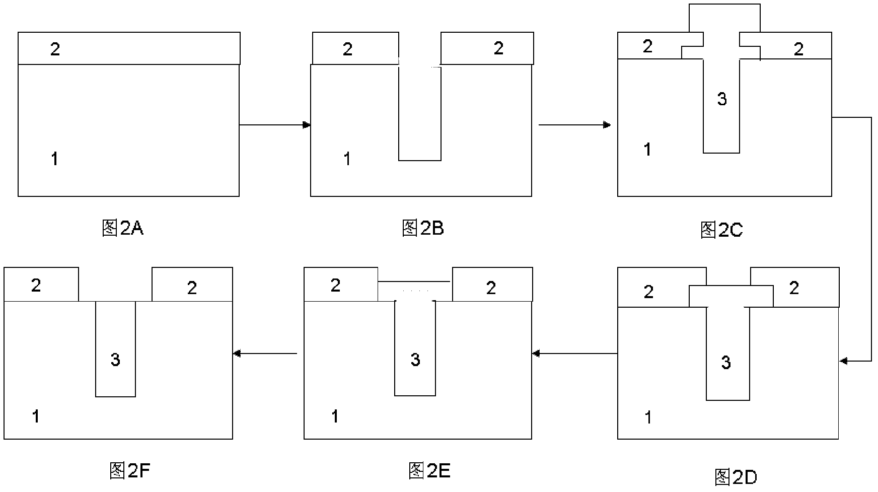
[0030] The invention provides a method for removing silicon ridges produced during the epitaxial deposition of super junction high-voltage devices, so as to remove single crystal silicon in the bottom cut caused by the introduction of etching gas in the oxide layer during the epitaxial process the goal of. Such as figure 1 with figure 2 Shown, the inventive method specifically comprises the following steps:

[0031] Step 1. If figure 2 Shown in A, deposit oxide film and / or nitride film 2 on the silicon chip surface (i.e. silicon substrate 1), the thickness of oxide layer or nitride film is 1000~1500 angstroms, and its technology used can be LPCVD process ( Low pressure chemical vapor deposition process), or PECVD process (plasma chemical vapor deposition process).

[0032] Step 2. If figure 2 As shown in B, a deep trench is etched on ...


PUM

PropertyMeasurementUnit
thicknessaaaaaaaaaa
depthaaaaaaaaaa
widthaaaaaaaaaa

Abstract

The invention discloses a method for removing silicon ridge produced in epitaxial deposition of a super-junction high-pressure device. The method includes the steps of firstly, depositing a layer of oxide film and / or nitride film on the surface of a silicon chip; secondly etching a deep groove on the silicon chip; thirdly, filling the deep groove with monocrystalline silicon or polycrystalline silicon; fourthly, performing planarization to the surface of the silicon chip by chemical mechanical grinding process, and using the oxide film and / or nitride film as a grinding retaining layer; fifthly, performing back-etching to the part of the oxide film and / or nitride film on two sides of the deep groove by etching process to expose the silicon ridge; and sixthly, etching the silicon ridge to remove by the etching process. The monocrystalline silicon in a bottom cut produced in an oxidation layer due to the fact that etching gas is guided in the epitaxial process can be removed, and accordingly the following gate polycrystalline silicon and the gate oxidation layer are provided with fine surface appearance, the following processes can be prevented from influence of the silicon ridge and certain electric performance of the device is free of influence.

Description

technical field [0001] The invention belongs to the manufacturing process of semiconductor integrated circuits, in particular to a preparation process of a super-junction high-voltage device structure, and in particular to a method for removing silicon ridges produced during the epitaxial deposition process of the super-junction high-voltage device. Background technique [0002] In today's semiconductor technology, deep trench structures are widely used. For example, it is used as an isolation structure to isolate electronic devices with different operating voltages, and it is used in super junction structure semiconductor devices as a P-N junction to achieve high breakdown voltage performance through charge balance in the depletion state, etc. For the latter super junction metal oxide semiconductor field effect transistor, the method of etching and filling the deep trench in the manufacturing process of the super junction MOS transistor is usually: growing a layer of n-type...

Claims


Application Information

Patent Timeline
Patent Type & Authority Applications(China)
IPC IPC(8): H01L21/336
Inventor 钱志刚程晓华
Owner SHANGHAI HUAHONG GRACE SEMICON MFG CORP
Why Eureka
Try Eureka