
Manufacturing method of semiconductor device composed of integrated circuit

A manufacturing method and integrated circuit technology, applied in semiconductor/solid-state device manufacturing, semiconductor devices, electric solid-state devices, etc., can solve the problems of fine dispersion of precipitated phases, unsatisfactory comprehensive properties of copper-iron alloys, uneven alloy structure, etc., to achieve The effect of fine dispersion of precipitated phase, excellent hot workability and low alloy price

Inactive Publication Date: 2013-03-20
JIANGSU WINAD LIGHTING TECH
View PDF4 Cites 0 Cited by
  • Summary
  • Abstract
  • Description
  • Claims
  • Application Information

AI Technical Summary

Problems solved by technology

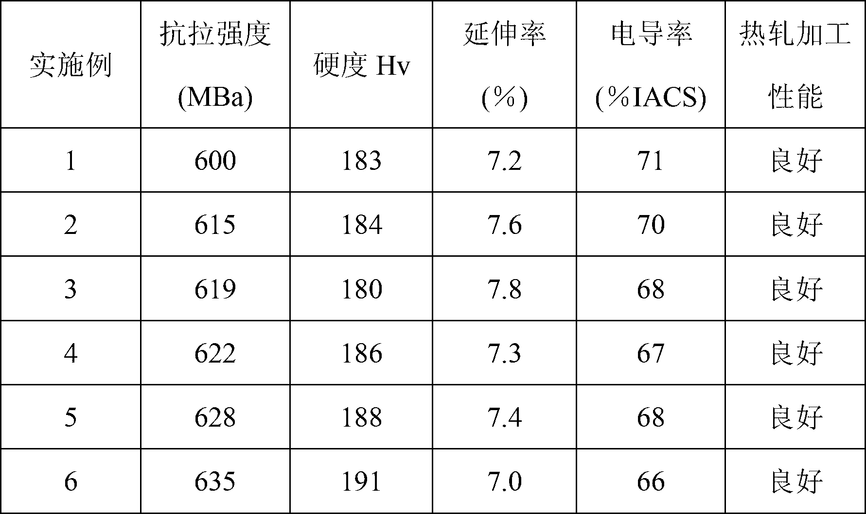
[0005] The invention provides a method for manufacturing a semiconductor device, which includes manufacturing an integrated circuit, wherein the method for manufacturing a copper-iron alloy for a lead frame of an integrated circuit can effectively solve the problem that the comprehensive performance of the copper-iron alloy used for a lead frame does not meet the production requirements, and the alloy structure is not satisfactory. Uniformity, fine dispersion of precipitated phases, etc., the tensile strength, hardness, elongation, electrical conductivity, and softening temperature of the copper-iron alloy prepared by the manufacturing method of the present invention can better meet the requirements of lead frame materials in the field of electronics industry. performance requirements

Method used


Image

  • Manufacturing method of semiconductor device composed of integrated circuit
  • Manufacturing method of semiconductor device composed of integrated circuit

Examples


Embodiment

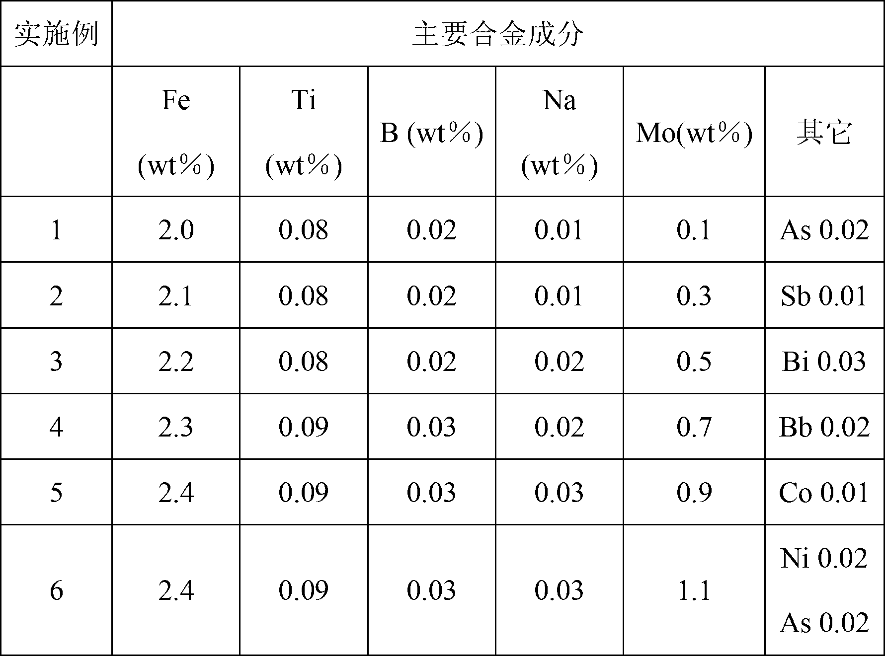
[0054] The copper-iron alloy No. 1~6 of composition (wt%) shown in table 1,

[0055] Table 1

[0056]

[0057] It is worth noting that during the melting process of the alloy, each element has different degrees of burning loss, and the burning loss rate is Fe: 1-2%, Ti: 1-3%, B: 2-5%, Na: 20 ~30%, Mo: 30~50%; it should be supplemented during the batching process. At the beginning of smelting, add electrolytic copper and copper-iron intermediate alloy first, start heating, and after it melts, add 1 / 3 of copper-boron intermediate alloy and keep it warm for 1 to 3 minutes; then add titanium, sodium and rare earth, and keep it warm for 3 minutes after melting ~5min, then add the remaining 2 / 3 of the copper-boron intermediate alloy, and cast it with heat preservation for 10min after full melting; use a small vertical semi-continuous casting machine to cast a billet of 70×180×1000 (mm), and use the billet mold for one cooling and Water shower is used for secondary cooling, so t...


PUM


Abstract

The invention discloses a manufacturing method of a semiconductor device composed of an integrated circuit. The manufacturing method comprises that the integrated circuit is manufactured and packed in a sealing mode, wherein the manufacture of the integrated circuit comprises that a chip is provided and fixed; a leading wire support is manufactured; the leading wire is drawn off and packed in a sealing mode, wherein the manufacture of the leading wire support comprises casting, injection of a blank mold and cooling. A casting blank is hot rolled and calendared. Hot rolled strip materials are repeatedly cool rolled, calendared and two-stage continuous annealed. Cool rolling and calendaring processes enable the variable quantity of thickness of the strip materials to reach more than 40%. The strip materials are annealed in a low temperature, and therefore finished products of the strip materials are obtained. Component contents are controlled in a manufacturing process, wherein ferrum is controlled between 2.0 wt % and 2.6 wt %, titanium is controlled between 0.05 wt % and 0.1 wt %, boron is controlled between 0.01 wt % and 0.03 wt %, sodium is controlled between 0 and 0.05 wt %, molybdenum is controlled between 0.01 wt % and 1.5 wt %, and the rest are cuprum and impurity substance. According to the manufacturing method, alloy structure of a cuprum and ferrum alloy has the advantages of being even, tiny and dispersive in precipitated phase, high in tensile strength, good in hardness, high in conductivity and ductility and capable of meeting the requirements of performance of leading wire frame materials in an electronic industry field.

Description

technical field [0001] The invention relates to a manufacturing method of a semiconductor device, in particular to a manufacturing method of a semiconductor device composed of an integrated circuit with a lead frame. Background technique [0002] At present, the electronic information industry has become an important pillar industry in my country. As the cornerstone of this pillar industry, semiconductor devices include external packaging and internal integrated circuits; integrated circuits (IC) include chips, leads and lead brackets, adhesive materials, packaging materials etc. Among them, the main function of the lead frame is to provide a mechanical support carrier for the chip, and it also has the functions of connecting external circuits, transmitting electrical signals, and dissipating heat. Therefore, IC packaging needs to have comprehensive properties such as high strength, high electrical conductivity, high thermal conductivity, and good solderability, corrosion re...

Claims


Application Information

Patent Timeline
IPC IPC(8): H01L21/48H01L21/60H01L21/50C22C9/00C22F1/08
CPCH01L2924/0002H01L2924/00
Inventor 虞浩辉周宇杭
Owner JIANGSU WINAD LIGHTING TECH
Learn More