
Manufacturing method of copper-indium-gallium-selenium-sulfur five-element target material

A technology of copper indium gallium selenide sulfur and its production method, which is applied in the field of production of copper indium gallium selenide sulfur quinary targets, can solve the problems of reducing the conversion efficiency of solar cells, the inability to use DC sputtering, and complicated manufacturing processes, etc.

Inactive Publication Date: 2012-05-23
HELIOHAWK OPTOELECTRONICS CORP
View PDF5 Cites 4 Cited by
  • Summary
  • Abstract
  • Description
  • Claims
  • Application Information

AI Technical Summary

Problems solved by technology

[0004] In CIGS solar cells, the key lies in the process of making CIGS or CIGS thin films. In the common manufacturing process of CIGS thin films, since gallium is converted into a liquid state at 30°C, usually Copper-gallium alloy targets, copper-indium alloy targets or copper-indium-gallium alloy targets are formed by powder metallurgy, and after sputtering, they are selenized or vulcanized. Because selenization or vulcanization needs to be poisonous to the human body, such as Hydrogen selenide, hydrogen sulfide, or selenium vapor have potential industrial safety hazards in the process of manufacturing and mechanical maintenance, and it takes a long time and the utilization rate of materials is not high, making the manufacturing cost expensive. In addition, after selenization Step or sulfide copper indium gallium selenide or copper indium gallium selenide sulfur thin film, in which the composition and crystal phase of copper, indium, gallium, selenium and sulfur are not uniform, and there are often Cu on the grain boundary x Se, In 2 Se 3 and other miscellaneous items, resulting in poor yield rate, thereby reducing the conversion efficiency of solar cells
[0005] For the above shortcomings, the production of copper indium gallium selenide target material has become the key at present. At present, copper, indium gallium, selenium, and target nanopowder are first ground, pressed and sintered into the target material by powder metallurgy, but the grinding may The problem of impurity mixing occurs. Because the target material of this form is not combined, it is easy to segregate during the sputtering process, so that the composition changes with the use time, and the reproducibility of the film quality is not good. In addition, there are three compounds (Cu 2 Se, Ga 2 Se 3 、In 2 Se 3 ) in an oxygen-free environment with a planetary ball mill (planetary ball mill) high-energy grinding and then sintering, but this method needs to produce three or more alloys or compound powders, and the process is complicated. Currently, for five-element targets In addition, the target material produced by this method has the problem of poor conductivity, which makes it only suitable for radio frequency sputtering, but cannot be used for DC sputtering, so the production time is long and the efficiency is not good.

Method used


Image

  • Manufacturing method of copper-indium-gallium-selenium-sulfur five-element target material
  • Manufacturing method of copper-indium-gallium-selenium-sulfur five-element target material
  • Manufacturing method of copper-indium-gallium-selenium-sulfur five-element target material

Examples


Embodiment Construction

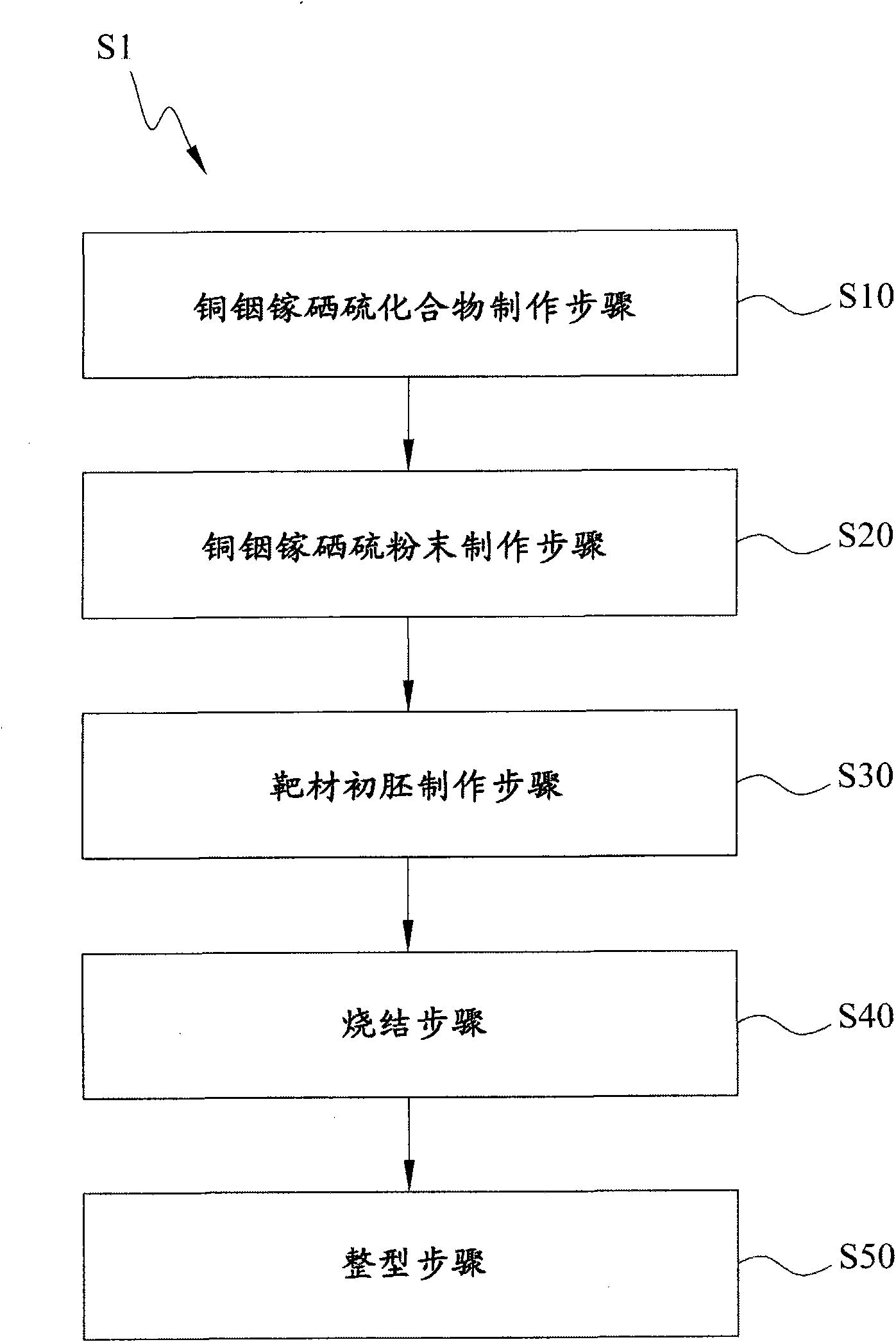
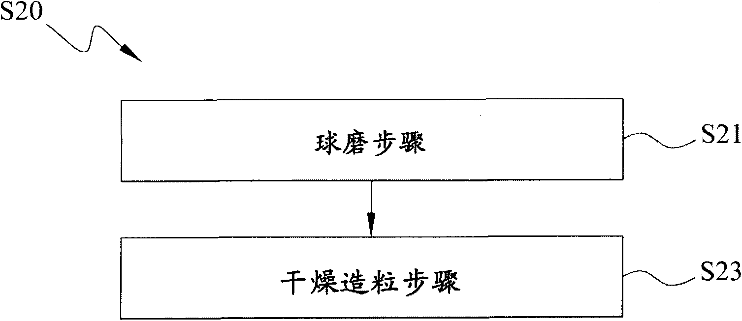
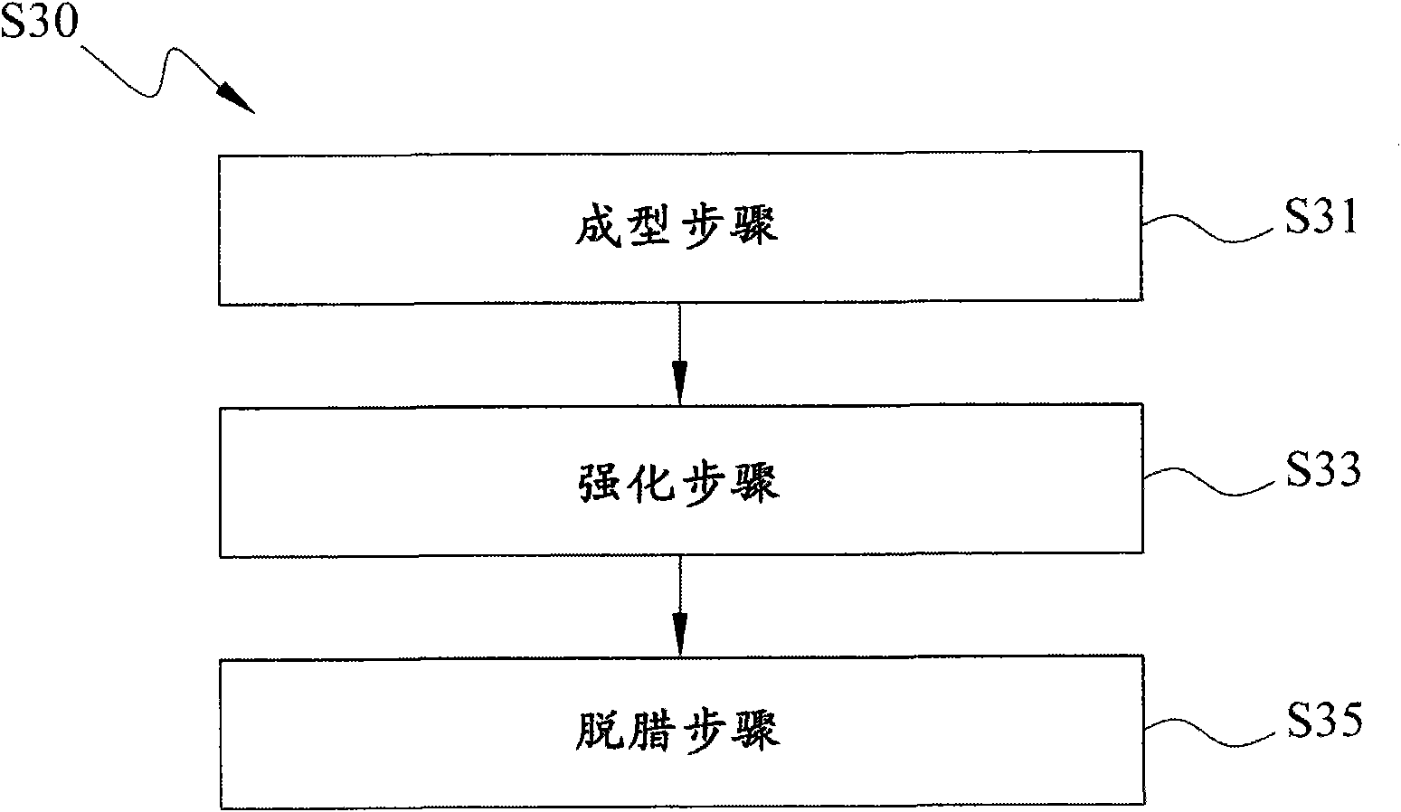
[0037] The implementation of the present invention will be described in more detail below with reference to the drawings and component symbols, so that those skilled in the art can implement it after studying this specification. figure 1 It is a flow chart of the first embodiment of the manufacturing method of the copper indium gallium selenium sulfur quinary target of the present invention. refer to figure 1 The manufacturing method S1 of the copper indium gallium selenide sulfur quinary target of the present invention comprises the manufacturing step S10 of the copper indium gallium selenide sulfur compound, the manufacturing step S20 of the copper indium gallium selenium sulfur powder, the manufacturing step S30 of the initial embryo of the target material, the sintering step S40 and the whole type step S50.

[0038] Copper indium gallium selenide sulfur compound production step S10 is mainly to mix copper, indium, gallium, selenium and sulfur element powders with a synthe...


PUM

PropertyMeasurementUnit
particle diameteraaaaaaaaaa
boiling pointaaaaaaaaaa

Abstract

The invention relates to a manufacturing method of a copper-indium-gallium-selenium-sulfur five-element target material. The manufacturing method comprises a manufacturing step of a copper-indium-gallium-selenium-sulfur compound, the manufacturing step of copper-indium-gallium-selenium powder, the manufacturing step of an initial billet of the target material, a sintering step and a shaping step, and the main process is as follows: mixing copper, indium, gallium, selenium and sulfur element powders through a synthetic solvent according to the atomic ratio, further synthesizing the copper-indium-gallium-selenium-sulfur compound through reaction, further manufacturing a copper-indium-gallium-selenium target material or mixing three-element or four-element compound powder as a precursor of the five-element target material in a mixing step, and performing high-pressure sintering. The copper-indium-gallium-selenium-sulfur five-element material is used for manufacturing a copper-indium-gallium-selenium thin film, then selenizing and sulfurizing steps can be omitted, and the safety in process is thus ensured; and furthermore, the conductivity of the target material is suitable for direct current sputtering and radio frequency sputtering, so that the sputtering efficiency can be upgraded and the copper-indium-gallium-selenium-sulfur thin film with no pollution and uniform components is formed.

Description

technical field [0001] The invention relates to a copper indium gallium selenium sulfur quinary target material, in particular to a manufacturing method of a copper indium gallium selenide sulfur quinary target material. Background technique [0002] In recent years, due to the rise of environmental protection awareness, countries have invested a lot of resources to develop solar cells. Among many solar cells, although silicon solar cells have better photoelectric conversion efficiency and mature manufacturing technology, the mass production scale of terminal silicon solar cells is considerably restricted due to insufficient supply of silicon wafers as upstream raw materials. Although dye-sensitized solar cells have lower manufacturing costs and do not suffer from the global shortage of silicon wafers because they do not require silicon wafers, they require specific photosensitizing dyes, and only a few manufacturers can supply them, so dye-sensitized solar cells are still ...

Claims


Application Information

Patent Timeline
Patent Type & Authority Applications(China)
IPC IPC(8): B22F3/16C23C14/34
CPCC23C14/0623C23C14/3414
Inventor 钟润文
Owner HELIOHAWK OPTOELECTRONICS CORP
Learn More