
Method for activating dopant atoms

A silicon wafer, polysilicon gate technology, applied in electrical components, semiconductor/solid-state device manufacturing, circuits, etc., can solve problems such as increased resistance, reduced device performance, and reduced proportions

Active Publication Date: 2013-11-20
SEMICON MFG INT (SHANGHAI) CORP +1
View PDF7 Cites 0 Cited by
  • Summary
  • Abstract
  • Description
  • Claims
  • Application Information

AI Technical Summary

Problems solved by technology

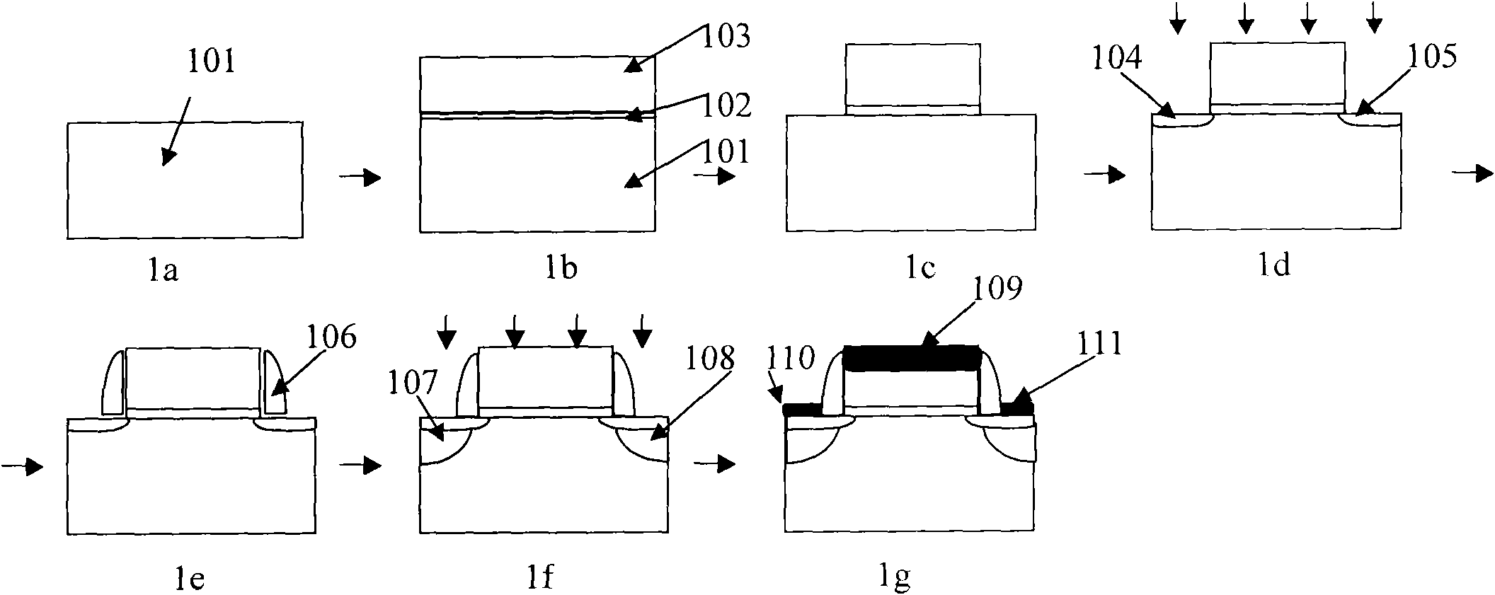
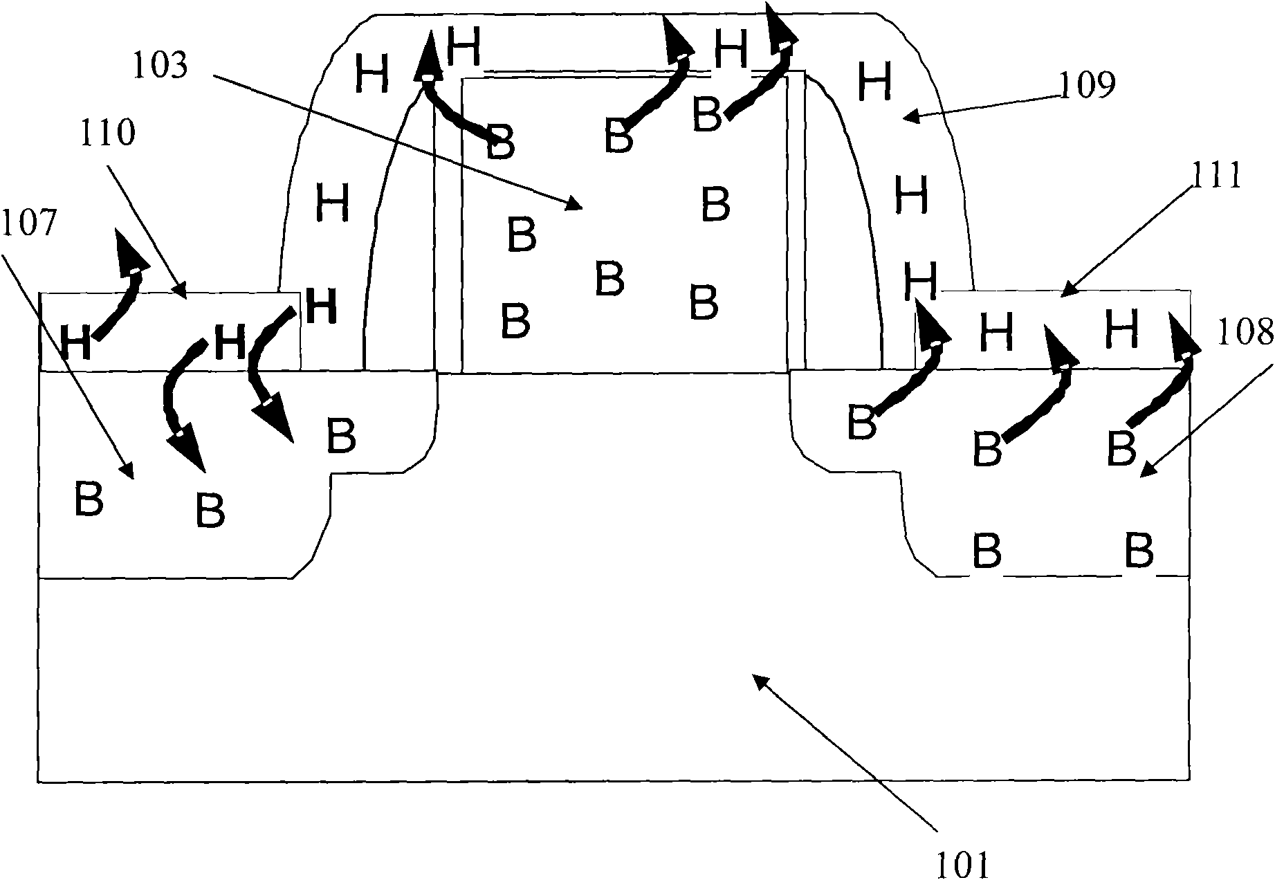
The final effect of the above effects is that the proportion of activated boron atoms in all doped boron atoms is significantly reduced, the resistance between the source 107 and the drain 108 increases, and the device performance is reduced.

Method used


Image

  • Method for activating dopant atoms
  • Method for activating dopant atoms
  • Method for activating dopant atoms

Examples


Embodiment Construction

[0036] The embodiment method of the present invention adopts nitrogen gas (N 2 ) or nitrogen oxides (N 2 O) and other nitrogen-rich gas plasmas are used to process silicon wafers, with the ultimate goal of suppressing the diffusion of boron atoms. During the above-mentioned plasma treatment process, a saturated and stable silicon-nitrogen bond compound is formed on the surface of the silicon wafer as a passivation layer. This layer of passivation layer can act as a protective layer to prevent the hydrogen atoms in the SAB layer from combining with the boron atoms in the source / drain, thus preventing the deactivation of the boron atoms and increasing the proportion of activated boron atoms.

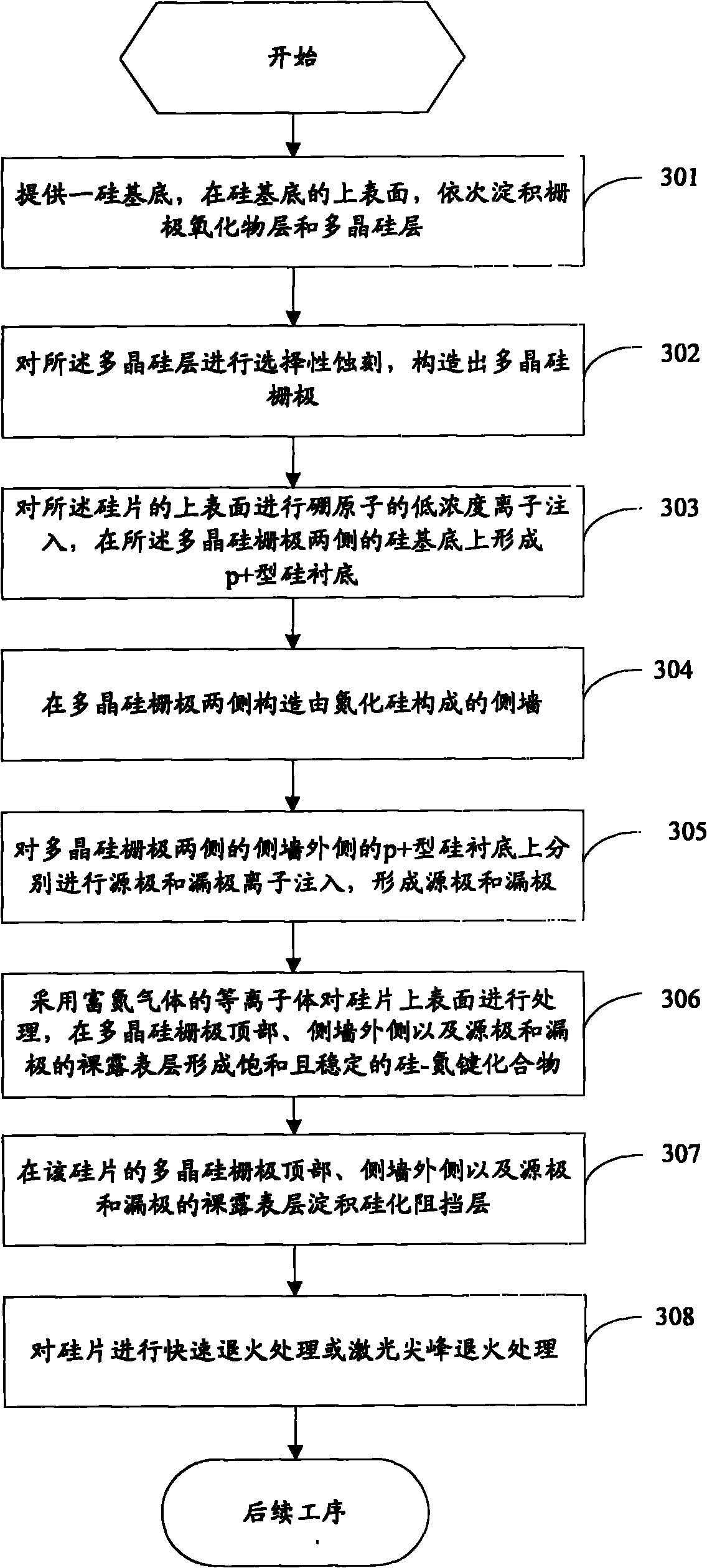
[0037] In the CMOS manufacturing process proposed by the embodiment of the present invention, the processing flow from the initial silicon substrate to the deposition of the silicide barrier layer is as follows: image 3 shown, including the following steps:

[0038] Step 301: providing...


PUM

PropertyMeasurementUnit
thicknessaaaaaaaaaa

Abstract

The invention provides a method for activating dopant atoms, which includes steps of making a polycrystalline silicon grid on a silicon base of a silicon chip, performing low-concentration ion implantation of boron atoms to the upper surface of the silicon chip to form a P+ type silicon substrate on the silicon base on two sides of the polycrystalline silicon grid, making side walls consisting of silicon nitride on two sides of the polycrystalline silicon grid, performing source electrode and drain electrode ion implantation on the P+ type silicon substrate on the outer sides of the side walls on two sides of the polycrystalline silicon grid to form a source electrode and a drain electrode, processing the upper surface of the silicon chip by plasmas of nitrogen-enriched gas to form saturated and stable silicon-nitrogen bond compound on bare surfaces of the source electrode, the drain electrode, the outer sides of the side walls and the top of the polycrystalline silicon grid, depositing silicified retaining layers on the bare surfaces of the source electrode, the drain electrode, the outer sides of the side walls and the top of the polycrystalline silicon grid of the silicon chip, and annealing the silicon chip. The method can effectively increase proportion of activated boron atoms.

Description

technical field [0001] The invention relates to the technical field of semiconductor integrated circuit manufacturing, in particular to a method for activating dopant atoms. Background technique [0002] The main raw material of semiconductor integrated circuit devices manufactured on a large scale at present is silicon. Intrinsic silicon has poor electrical conductivity, and only when a small amount of impurities are added to silicon to change its structure and electrical conductivity, silicon becomes a useful semiconductor. This process is called doping. Silicon doping is the basis for preparing pn junctions in semiconductor devices. [0003] Silicon chips need to be doped with Group IIIA (such as boron, aluminum, gallium, etc.) and Group VA impurities (such as phosphorus, arsenic, etc.). The focus of doping on silicon wafers lies in the profile of the device after each step of the process. Since the silicon wafer has to undergo multiple high-temperature processes in a...

Claims


Application Information

Patent Timeline
Patent Type & Authority Patents(China)
IPC IPC(8): H01L21/02H01L21/336
Inventor 李敏
Owner SEMICON MFG INT (SHANGHAI) CORP
Learn More