In, nb co-doped ZNO-based transparent conductive film and preparation method thereof
A transparent conductive film, co-doping technology, used in ion implantation plating, metal material coating process, coating and other directions
- Summary
- Abstract
- Description
- Claims
- Application Information
AI Technical Summary
Problems solved by technology
Method used
Image

Examples
Embodiment 1
[0020] A preparation method of In, Nb co-doped ZnO-based transparent conductive film:
[0021] (1) Prepare In and Nb co-doped ZnO targets, the target size is 30mm in diameter, 3mm in thickness, and the target is made of 1.0wt% In 2 o 3 +2.0wt%Nb 2 o 5 It is ground and mixed with ZnO powder, pressed into shape, and then sintered at 1200°C. Actual weighing: In 2 o 3 0.2577g, Nb 2 o 5 is 0.5155g, and ZnO is 25g.
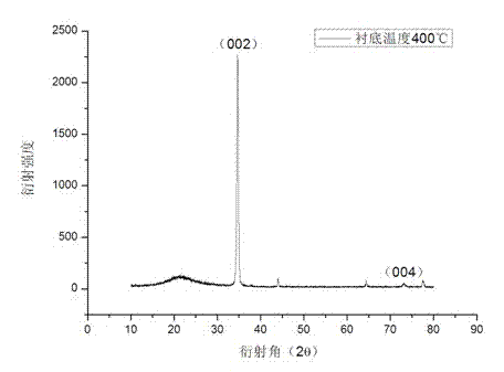
[0022] (2) Put the In and Nb co-doped ZnO target prepared in step 1, and the quartz wafer substrate cleaned with ultrasonic waves and acetone into the growth chamber of the pulsed laser deposition device, and the distance between the target material and the quartz wafer substrate The distance between them is 4cm, and the vacuum degree of the growth chamber is pumped to a pressure of 8×10 -4 Pa, the substrate temperature is 400°C, oxygen with a purity of 99.99% is introduced into the growth chamber, and the oxygen partial pressure is 6pa, the laser is turned on...
Embodiment 2
[0025] The preparation method is the same as that in Example 1, except that it is grown on a glass substrate. The resistivity of the In and Nb co-doped ZnO-based transparent conductive film prepared in this example is 9.2×10 -4 Ω·cm, the average light transmittance in the visible region is higher than 87%. After standing for several months, the photoelectric properties of the film did not change significantly.
Embodiment 3
[0027] A preparation method of In, Nb co-doped ZnO-based transparent conductive film:
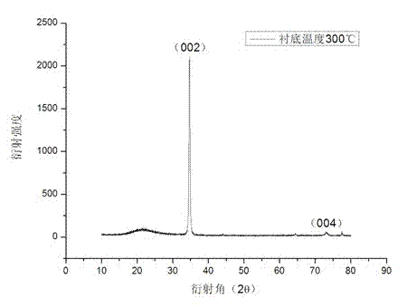
[0028] (1) Prepare In and Nb co-doped ZnO targets, the target size is 30mm in diameter, 3mm in thickness, and the target is made of 1.5wt%In 2 o 3 +2.0wt%Nb 2 o 5 It is ground and mixed with ZnO powder, pressed into shape, and then sintered at 1250°C. Actual weighing: In 2 o 3 0.3886g, Nb 2 o 5 is 0.5155g, and ZnO is 25g.
[0029] (2) Put the In and Nb co-doped ZnO target prepared in step 1, and the quartz wafer substrate cleaned with ultrasonic waves and acetone into the growth chamber of the pulsed laser deposition device, and the distance between the target material and the quartz wafer substrate The distance between them is 4.5cm, and the vacuum degree of the growth chamber is pumped to a pressure of 8×10 -4Pa, the substrate temperature is 300°C, oxygen with a purity of 99.99% is introduced into the growth chamber, and the oxygen partial pressure is 6pa, the laser is turned on...
PUM
| Property | Measurement | Unit |
|---|---|---|
| electrical resistivity | aaaaa | aaaaa |
| electrical resistivity | aaaaa | aaaaa |
| diameter | aaaaa | aaaaa |
Abstract
Description
Claims
Application Information
 - Generate Ideas
- Intellectual Property
- Life Sciences
- Materials
- Tech Scout
- Unparalleled Data Quality
- Higher Quality Content
- 60% Fewer Hallucinations
Browse by: Latest US Patents, China's latest patents, Technical Efficacy Thesaurus, Application Domain, Technology Topic, Popular Technical Reports.
© 2025 PatSnap. All rights reserved.Legal|Privacy policy|Modern Slavery Act Transparency Statement|Sitemap|About US| Contact US: help@patsnap.com