
Enhancement mode planar insulated gate bipolar transistor (IGBT)

A bipolar transistor, insulated gate technology, applied in semiconductor devices, electrical components, circuits, etc., can solve the problems of overvoltage and shock resistance, low anti-interference, high internal resistance of high-voltage IGBTs, and reduced voltage withstand capability of devices. Improve turn-off speed, reduce on-state voltage drop, and reduce the effect of on-state voltage drop

Inactive Publication Date: 2011-08-31
UNIV OF ELECTRONICS SCI & TECH OF CHINA +1
View PDF6 Cites 19 Cited by
  • Summary
  • Abstract
  • Description
  • Claims
  • Application Information

AI Technical Summary

Problems solved by technology

The biggest advantage of IGBT is that it can withstand the current impact no matter in the conduction state or in the short circuit state. Its disadvantage is that the internal resistance of the high-voltage IGBT is large, resulting in large conduction loss. Multiple in series, and low tolerance for overvoltage, overheating, impact resistance, anti-interference, etc.
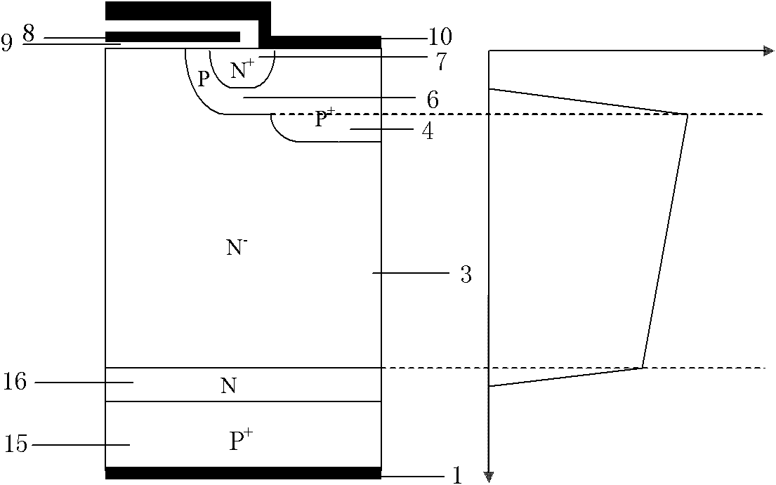
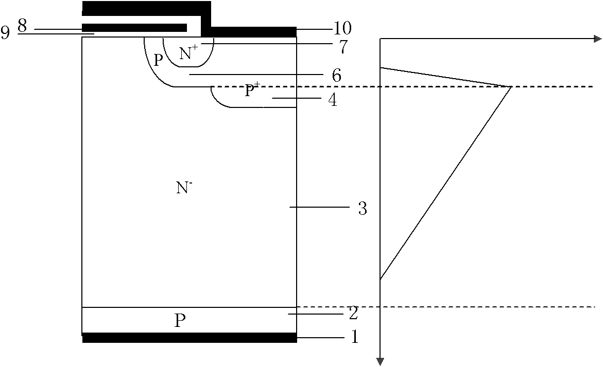
However, due to the concentration of the fully surrounded hole barrier layer 17 being higher than that of N - The drift region 3 is high, and the electric field will drop quickly in it, and the electric field distribution is as follows image 3 As shown, and the area of ​​the depletion region will be reduced during the withstand voltage of the device, causing the decline of the withstand voltage capability of the device; and the N-type hole barrier layer 17 and N - The built-in electric field formed by the drift region 3 will also prevent holes from flowing to the P-type base region 6 when the gate of the device is turned off, so that a large number of holes can only disappear through recombination, resulting in a prolonged turn-off time of the device; and when the device is turned on Once a large number of holes accumulated on the top of the device break through the hole barrier layer 17, it is very easy to cause latch-up of the device.

Method used


Image

  • Enhancement mode planar insulated gate bipolar transistor (IGBT)
  • Enhancement mode planar insulated gate bipolar transistor (IGBT)
  • Enhancement mode planar insulated gate bipolar transistor (IGBT)

Examples


Embodiment Construction

[0036] An enhancement mode planar insulated gate bipolar transistor, such as Figure 4 As shown, it includes the metallized collector electrode 1 on the back of the P-type collector region 2, the P-type collector region 2, and the N - The drift region 3 also includes a metallized emitter 10 located at N - N on top of drift region 3 and in contact with metallized emitter 10 + Type source region 7, N - Surrounded by N in drift region 3 + The P-type base region 6 of the type source region 7, the N - The N-type hole barrier layer 5 surrounding the P-type base region 6 in the drift region 3; the N-type hole barrier layers 5 of two adjacent cells are not connected. The metallized emitter 10 is a slot-shaped metallized emitter, and its slot-shaped part passes through the N + type source region 7 and extends into the P-type base region 6; under the groove-type portion of the metallized emitter 10, there is also a P connected to the groove-type portion of the metallized emitter 10...


PUM


Abstract

The invention discloses an enhancement mode planar insulated gate bipolar transistor (IGBT), belonging to the technical field of semiconductor power devices, wherein a hole bypass structure consisting of a P+ body region and a trench-type metallization emitter is introduced based on the traditional enhancement mode planar IGBT; and on the basis of the traditional non-through type planar IGBT, a JFET(Junction Field Effect Transistor) effect weakening structure consisting of an N type hole potential barrier layer and an N- draft region is introduced, and a path structure of expanded current formed by the N type hole potential barrier layer is introduced. Through the N type hole potential barrier layer, the conductivity modulation effect of one side of a device near the emitter can be enlarged, the JFET effect is reduced, the area flown through by electronic current is increased, therefore the on-state voltage drop is lowered; through the trench-type hole bypass structure, the current density of a latch can be increased, hole extraction is accelerated, and then the shutoff speed is enhanced; in addition, the area of an exhaustion region is increased by the P+ body region, thus the breakdown voltage is also increased; and the resistance of the device can be further lowered by the trench-type metallization emitter, thus the on-state voltage drop is reduced.

Description

technical field [0001] The invention relates to an enhanced planar insulated gate bipolar transistor, which belongs to the technical field of semiconductor power devices. Background technique [0002] IGBT (Insulate Gate Bipolar Transistor) insulated gate bipolar transistor is a new type of power semiconductor device. It has become a new generation of mainstream products in the field of power electronics. It is a combination of MOS and bipolar devices with MOS input and bipolar output functions. Structurally, it is a high-power integrated device composed of thousands of repeating units (ie, cells) and manufactured using large-scale integrated circuit technology and power device technology. [0003] IGBT not only has the advantages of high input impedance, low control power, simple driving circuit and high switching speed of MOSFET, but also has the advantages of high current density, low saturation voltage and strong current handling capacity of bipolar power transistor. ...

Claims


Application Information

Patent Timeline
IPC IPC(8): H01L29/739H01L29/06
Inventor 李泽宏张超肖璇吴宽姜贯军余士江谢家雄
Owner UNIV OF ELECTRONICS SCI & TECH OF CHINA
Learn More