
LED (light-emitting diode) radiating substrate based on diamond film and manufacturing method thereof

A technology of diamond thin film and heat dissipation substrate, which is applied in the direction of electrical components, circuits, semiconductor devices, etc., can solve the problems of complex heat dissipation structure manufacturing process, small air thermal conductivity, and limited heat dissipation effect, so as to reduce transmission distance and junction thermal resistance , the effect of improving efficiency

Active Publication Date: 2011-07-20
TIANJIN UNIVERSITY OF TECHNOLOGY
View PDF6 Cites 19 Cited by
  • Summary
  • Abstract
  • Description
  • Claims
  • Application Information

AI Technical Summary

Problems solved by technology

The manufacturing process of this heat dissipation structure is complicated and the heat dissipation effect is limited due to the small thermal conductivity of air (0.023W / m·K).

Method used


Image

  • LED (light-emitting diode) radiating substrate based on diamond film and manufacturing method thereof
  • LED (light-emitting diode) radiating substrate based on diamond film and manufacturing method thereof
  • LED (light-emitting diode) radiating substrate based on diamond film and manufacturing method thereof

Examples


Embodiment 1

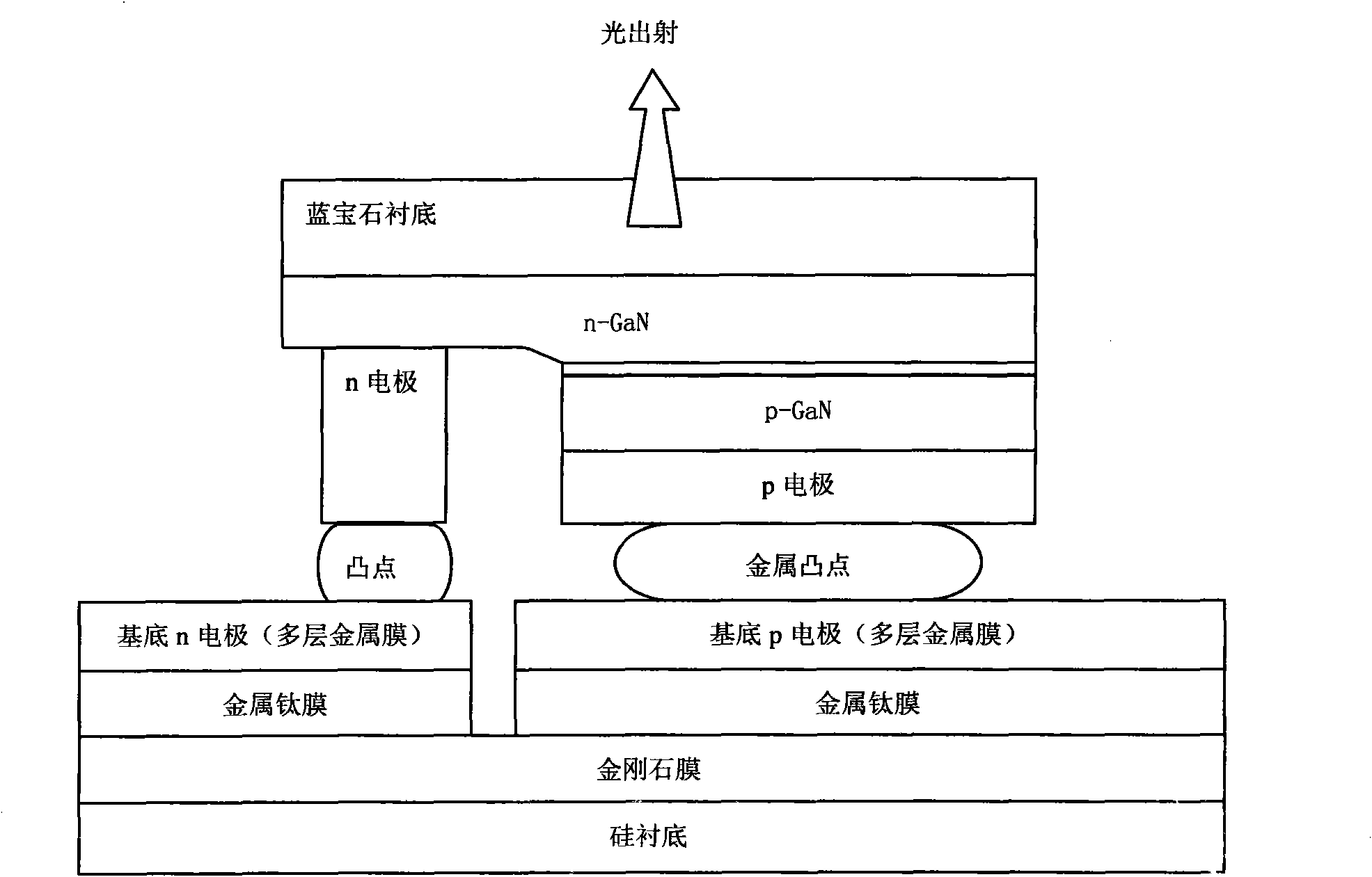
[0037] image 3 It is a cross-sectional view of the FC-LED structure using the DOS structure as the heat dissipation substrate in Embodiment 1, and its manufacturing process will be described in detail below.

[0038] The LED in Example 1 is a traditional GaN light-emitting diode with sapphire as the substrate. An epitaxial layer is grown on a sapphire substrate, and the epitaxial layer generally includes three layers: the upper layer is an n-GaN film, the lower layer is a p-GaN film, and the middle layer is an LED light-emitting active layer; a compound metal is deposited on the p-GaN of the epitaxial layer layer as a light-emitting reflective layer and electrode; etch away part of the p-type epitaxial layer and light-emitting active layer until the n-type layer is exposed, and then deposit an aluminum-based n-electrode contact on the exposed n-type GaN layer; on the p-type and n-type electrodes Make metal bumps for soldering.

[0039] The heat dissipation substrate for the...

Embodiment 2

[0048] Figure 4 It is a cross-sectional view of the TFFC-LED structure using DOS as the heat dissipation substrate in Embodiment 2, and the structure will be described in detail below.

[0049] Thin-film flip-chip LED structure (TFFC-LED) is to combine thin-film LED and flip-chip LED. The traditional LED substrate sapphire is removed with an excimer laser; the surface of the exposed n-type GaN layer is roughened with photoresist technology; then an n-type electrode is prepared on the n-GaN with a rough structure, and the wire Bond with the n-type electrode on the heat dissipation substrate, and finally connect the p-GaN of the vertical structure LED to another electrode of the heat dissipation substrate.

[0050] The manufacturing method of the heat dissipation substrate for the thin-film flip-chip LED structure is the same as that in Embodiment 1.

[0051] Flip-chip welding the prepared thin film LED to the prepared heat dissipation substrate. The flip-chip welding struct...


PUM

PropertyMeasurementUnit
thicknessaaaaaaaaaa

Abstract

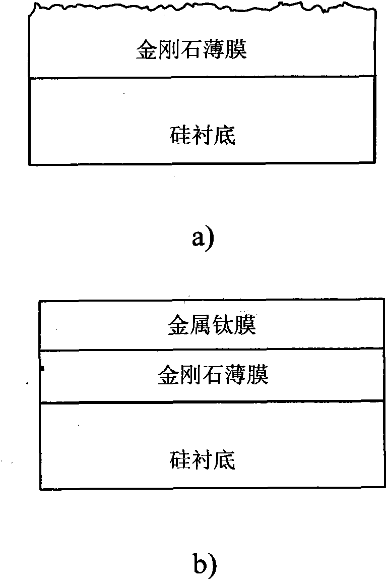
The invention relates to a radiating substrate based on a diamond film, comprising a silicon substrate, the diamond film and a transition layer, wherein the diamond film prepared on the silicon substrate has a diamond-on-silicon (DOS) structure; after an end-sealing top layer is removed and surface planarization is carried out, the roughness of the surface of the diamond film is at the nano orderand surface modification is carried out; and the transition layer is a Ti film, and is firstly deposited on the diamond film with a modified surface before metal bumps are prepared. The radiating substrate has the advantages that the diamond film with highest heat conductivity is adopted as a radiating layer of the LED (light-emitting diode) base to form the DOS structure, so that the radiating efficiency is greatly improved; simultaneously, the metal bumps for welding are directly manufactured on a radiating sink, so that the heat transfer distance is shortened; the thermochemical and mechanical planarization is utilized for carrying out surface modification and planarization on the surface of a diamond, so that the roughness of the surface is improved, and the valence bonds of the surface are activated, so that the adhesion among the diamond film and the metal bumps is improved, and the defects of generating air bubbles in the middle of a contact interface and the like are prevented; and due to the formed good contact interface, the heating resistance can be reduced and the radiating efficiency can be improved.

Description

(1) Technical field [0001] The invention relates to the cross-technical field of optoelectronic device packaging and materials, in particular to a heat dissipation substrate based on a diamond film and a manufacturing method thereof. (2) Background technology [0002] Light-emitting diode (LED) is a light-emitting element that directly converts electrical energy into light energy. It has many advantages that traditional light sources do not have, such as: better driving characteristics, faster response speed, higher shock resistance, longer Long service life, green environmental protection and other advantages. However, low luminous efficiency and high cost limit its wide application in the lighting field. With the continuous development of LED chip manufacturing technology and packaging technology, LED has been continuously improving brightness along Haitz's law (Moore's law in the LED industry) in recent years. cut costs. People began to pay attention to the application ...

Claims


Application Information

Patent Timeline
Patent Type & Authority Applications(China)
IPC IPC(8): H01L33/02H01L33/00
Inventor 张楷亮张涛峰王芳曲长庆王莎莎
Owner TIANJIN UNIVERSITY OF TECHNOLOGY
Learn More