Semiconductor storage device
A storage device and semiconductor technology, applied in the field of high speed, can solve the problems of increased area, increased gate capacitance, difficulty in adapting to high speed, etc., and achieves the effect of suppressing the increase in area
- Summary
- Abstract
- Description
- Claims
- Application Information
AI Technical Summary
Problems solved by technology
Method used
Image

Examples
Embodiment Construction
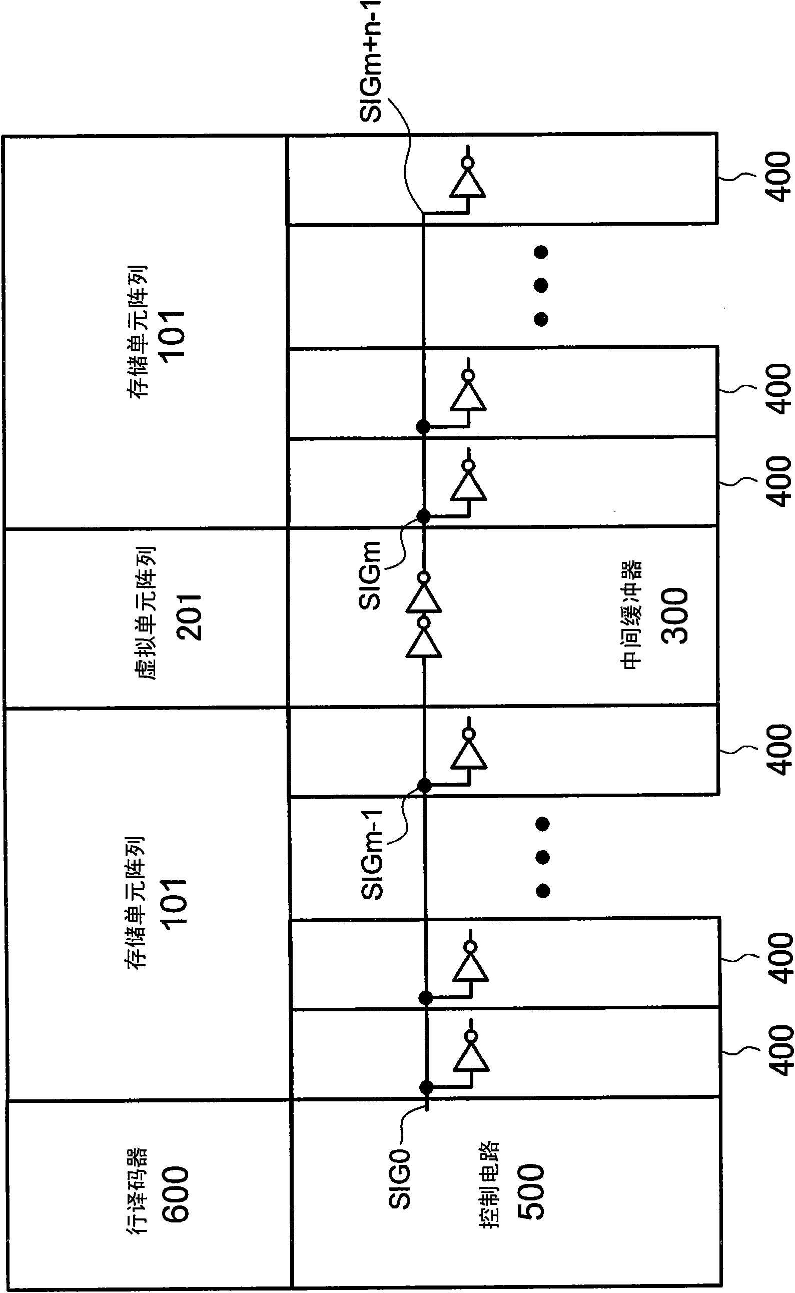
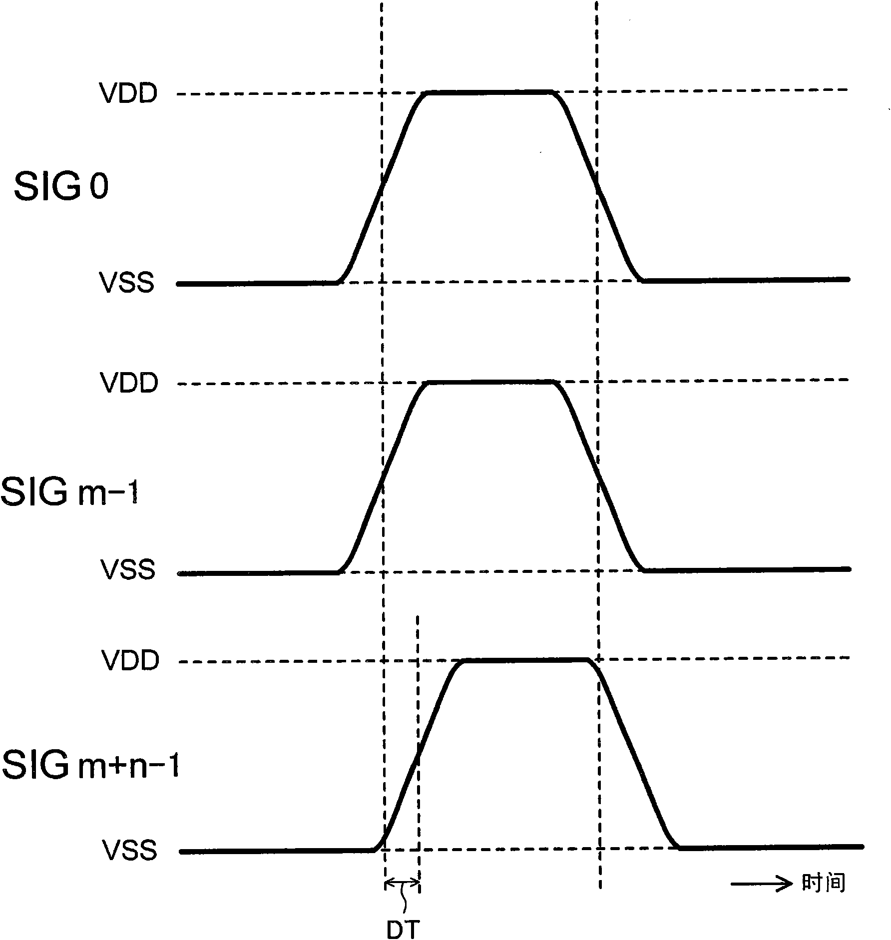
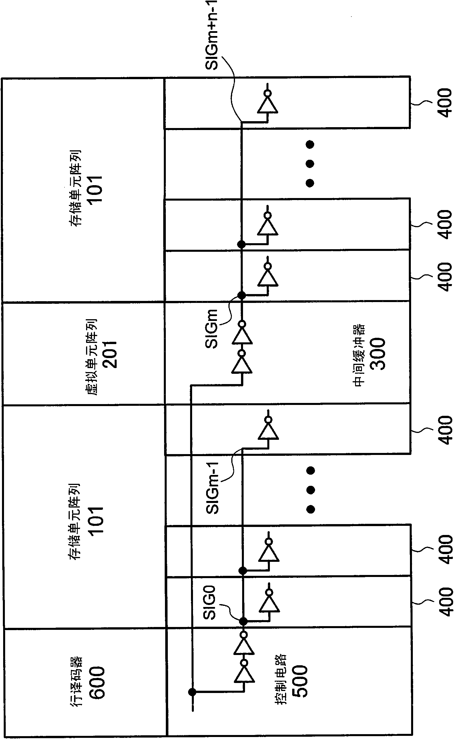
[0034] figure 1 It is a structural diagram of a semiconductor memory device in the embodiment of the invention, and is an m+n memory cell array 101, a dummy cell array 201, an intermediate buffer 300, an input / output circuit 400, a control circuit 500, and a row decoder 600. bit wide memory. The intermediate buffer 300 is disposed between the m-th bit input-output circuit 400 and the m+1-th bit input-output circuit 400, and at a position corresponding to the intermediate buffer 300 in the memory cell array 101, a A dummy cell array 201 in which dummy cells are arranged in a direction. SIG0 to SIGm+n−1 represent control signals of the input / output circuit 400 , and are nodes at the positions of the respective input / output circuits 400 . For example, a sense amplifier enable signal, a bit line precharge signal, a column decode signal, etc. correspond thereto. Since SIGm buffers SIGm-1 through the intermediate buffer 300, there are two levels of difference in the number of gat...
PUM
 Abstract
Description
Claims
Application Information
 - R&D
- Intellectual Property
- Life Sciences
- Materials
- Tech Scout
- Unparalleled Data Quality
- Higher Quality Content
- 60% Fewer Hallucinations
Browse by: Latest US Patents, China's latest patents, Technical Efficacy Thesaurus, Application Domain, Technology Topic, Popular Technical Reports.
© 2025 PatSnap. All rights reserved.Legal|Privacy policy|Modern Slavery Act Transparency Statement|Sitemap|About US| Contact US: help@patsnap.com