Dynamic semiconductor memory and semiconductor IC device
A technology of integrated circuits and semiconductors, applied in the field of improvement of refresh actions, can solve problems such as the impact of DRAM system performance, and achieve the effects of lightening load, improving system performance, and reducing occurrence frequency
- Summary
- Abstract
- Description
- Claims
- Application Information
AI Technical Summary
Problems solved by technology
Method used
Image

Examples
Embodiment 1
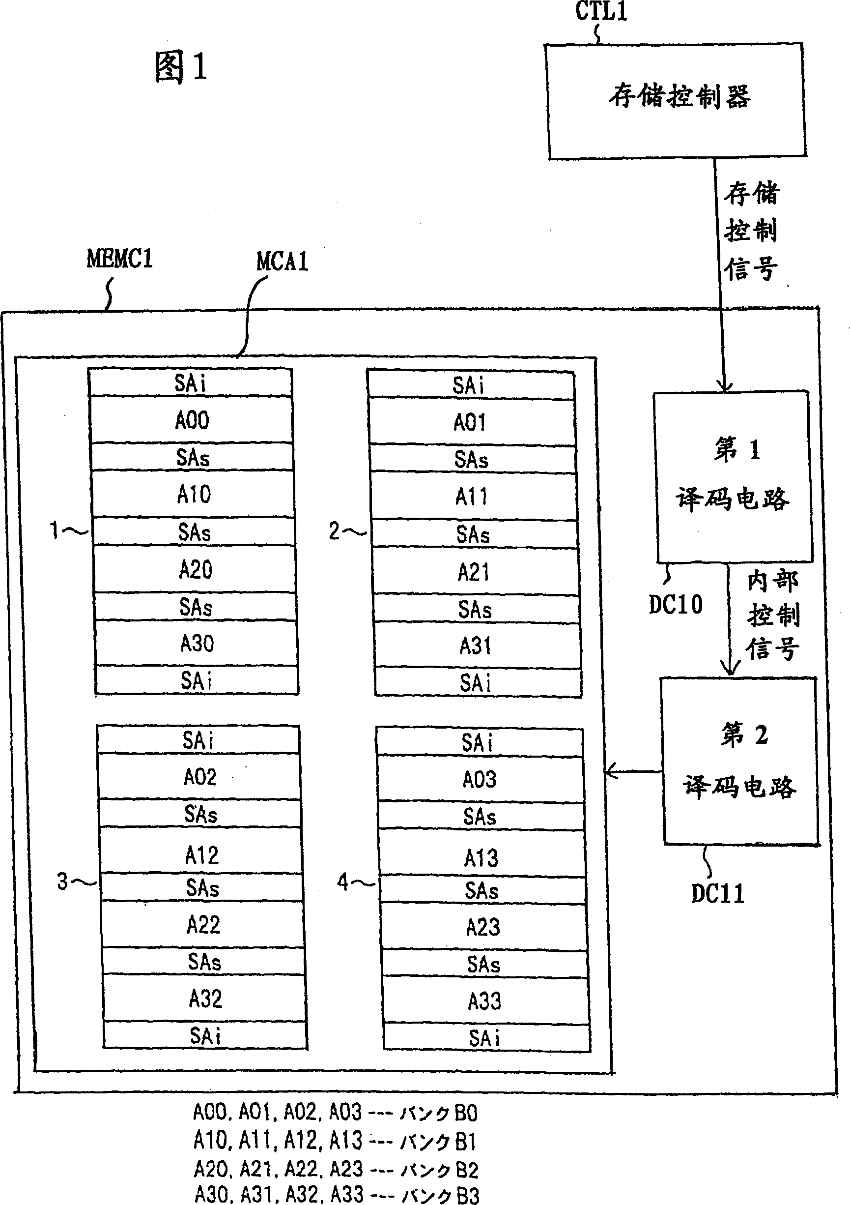
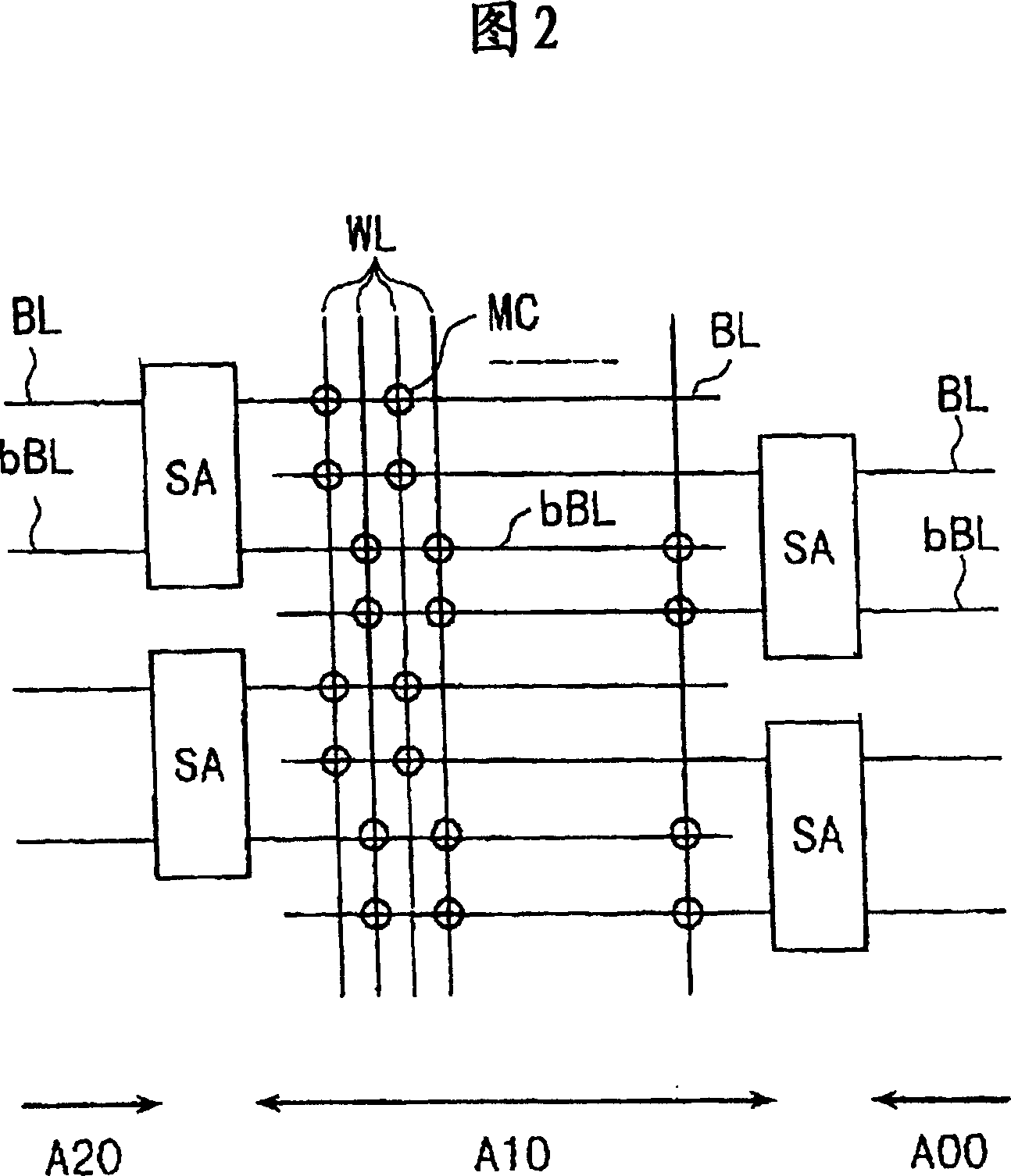
[0054] FIG. 1 shows a memory cell array of a DRAM according to the first embodiment. In Embodiment 1, each of the 16 sub-arrays constitutes one memory bank, which is an example of the structure of four memory banks. Specifically, every four sub-arrays (A00, A10, A20, A30), (A01, A11, A21, A31), (A02, A12, A22, A32), (A03, A13, A23, A33), respectively in phase The sense amplifier circuit SAs is shared between adjacent sub-arrays to form memory blocks 1 , 2 , 3 , and 4 . Both ends of each of the memory blocks 1 to 4 have independent sense amplifier circuits SAi that are not shared with other subarrays.
[0055] In addition, in each of the following embodiments, the sense amplifier circuits shared by adjacent subarrays are shown as "SAs", and the sense amplifier circuits shared with other subarrays are shown as "SAi".
[0056] In each of the memory blocks 1 to 4, the first sub-arrays A00, A01, A02, and A03 constitute one bank B0. Similarly, the second sub-array A10, A11, A12 a...
Embodiment 2
[0077] FIG. 5 shows a circuit configuration of a second decoding circuit DC11 capable of simultaneously activating a plurality of sub-arrays at the time of refresh based on the DRAM cell array of FIG. 1 . A refresh control signal REFRESH, bank addresses bank0, bank1, and row addresses RAD0, RAD1 are input from the first decoding circuit DC10 to the second decoding circuit DC11.
[0078] For each cell array storage block 1-4, there are decoding parts 411-414 for sub-array selection by means of bank addresses bank0 and bank1. The AND gates G00, G10, G20, and G30 of the decoding part 411 are respectively used to activate the sub-arrays A00, A10, A20, and A30 in the storage block 1, and perform "0" and "1" of the memory address bank0 and bank1. In the consistent detection of the "combination, only one output is active "H", and the decoding parts 412, 413, 414 of other storage blocks are also the same.
[0079] Furthermore, a decoding section 415 for selecting a memory block is pr...
Embodiment 3
[0087] FIG. 6A shows the structure of the memory cell array MCA2 in the memory chip MEMC2 of the third embodiment. In this embodiment, every two sub-arrays (A00, A01), (A10, A11), (A20, A21) and (A30, A31) constitute storage banks B0, B1, B2 and B3. Two sub-arrays for each bank are formed and arranged with sub-arrays of other banks sandwiched between them. In the bank, the two sub-arrays do not share a sense amplifier circuit. Independent sense amplifier circuits SAi that are not shared with the subarrays are disposed at both ends of the subarray arrangement.
[0088] In the case of this embodiment, for example, banks B1 and B3 are adjacent to bank B2 and share the sense amplifier circuit. Therefore, substantially the same non-standalone-bank DRAM structure as that of FIG. 1 is obtained.
[0089] In the case of this embodiment, in the row access mode, for example, when the bank B2 is selected, the activated bank is one of the sub-arrays A20 and A21. On the other hand, in th...
PUM
 Abstract
Description
Claims
Application Information
 - R&D
- Intellectual Property
- Life Sciences
- Materials
- Tech Scout
- Unparalleled Data Quality
- Higher Quality Content
- 60% Fewer Hallucinations
Browse by: Latest US Patents, China's latest patents, Technical Efficacy Thesaurus, Application Domain, Technology Topic, Popular Technical Reports.
© 2025 PatSnap. All rights reserved.Legal|Privacy policy|Modern Slavery Act Transparency Statement|Sitemap|About US| Contact US: help@patsnap.com