Latch circuit and semiconductor memory device

A latch circuit, oxide semiconductor technology, applied in static memory, read-only memory, information storage and other directions, can solve the problems of large circuit size, large current consumption, inability to achieve high-speed operation, etc., to achieve small circuit size and current consumption. small effect

Active Publication Date: 2020-08-04
POWERCHIP SEMICON MFG CORP
View PDF9 Cites 0 Cited by
  • Summary
  • Abstract
  • Description
  • Claims
  • Application Information

AI Technical Summary

Problems solved by technology

[0038] However, for example, in Patent Document 1 to Patent Document 3, although various conventional latch circuits are disclosed, there is a problem that the current consumption is relatively large, the circuit size is also large, and high-speed operation cannot be realized.

Method used


Image

  • Latch circuit and semiconductor memory device
  • Latch circuit and semiconductor memory device
  • Latch circuit and semiconductor memory device

Examples


Embodiment Construction

[0106] Hereinafter, embodiments of the present invention will be described with reference to the drawings. In addition, in each of the following embodiments, the same reference numerals are attached to the same components.

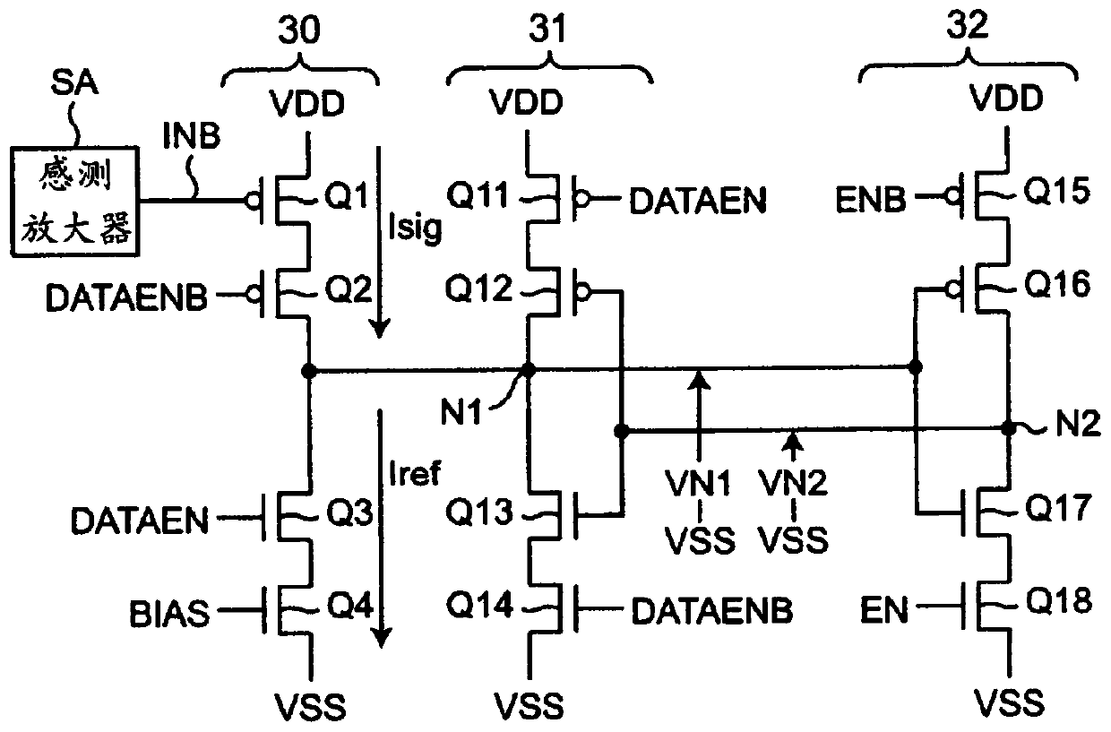
[0107] Figure 5 It is a circuit diagram showing a circuit configuration of a latch circuit of a flash EEPROM according to an embodiment of the present invention. Figure 5 The latch circuit compared to image 3 The latch circuit is different in the following respects.

[0108] (1) The reset signal RST is applied to the gate of the NMOS transistor Q3 instead of the data enable signal DATAEN.

[0109] (2) An NMOS transistor Q15 is connected in parallel with the NMOS transistor Q14 instead of the NMOS transistor Q4 , and the NMOS transistor Q15 controls the reference current corresponding to the bias voltage BIAS.

[0110] (3) The reset signal RST is applied to the gate of the PMOS transistor Q11 instead of the data enable signal DATAEN.

[0111] (4) Th...


PUM


Abstract

latch circuits and semiconductor memory devices. The latch circuit includes an input circuit including an input PMOS transistor that causes a signal current corresponding to the sensed voltage to flow; a first inverter including a first PMOS transistor, a first NMOS transistor, and a first node. The first PMOS transistor and the first NMOS transistor are connected and connected to the input circuit; and the second inverter includes a second PMOS transistor, a second NMOS transistor and a second node, the second node connects the second PMOS transistor and the second NMOS transistor. The first inverter and the second inverter are connected in cascade.

Description

technical field [0001] The present invention relates to a latch circuit for temporarily storing, for example, data read from the semiconductor memory device, and a semiconductor memory device including the latch circuit. The semiconductor memory device is an electrically rewritable nonvolatile semiconductor memory device (Electrically Erasable Programmable Read Only Memory, EEPROM) such as a flash memory (flash memory). Background technique [0002] There is known a kind of NOR (NOR) type nonvolatile semiconductor memory device (especially NOR type flash EEPROM), and it is connected in parallel between bit line (bit line) and source electrode line (source line) and multiple Each word line (word line) corresponds to a plurality of memory cell transistors (memory cell transistors) (hereinafter referred to as memory cells) to form a memory cell array (memory cell array) to achieve high integration. [0003] figure 1 It is a block diagram showing the overall structure of a con...

Claims


Application Information

Patent Timeline
Patent Type & Authority Patents(China)
IPC IPC(8): G11C16/06G11C16/26
CPCG11C16/06G11C16/26G11C16/30G11C16/08G11C16/10G11C16/14
Inventor 中山晶智
Owner POWERCHIP SEMICON MFG CORP
Why Eureka
Try Eureka