N-type single crystal silicon substrate PN junction inversion layer battery and manufacturing method thereof
A manufacturing method and technology of single crystal silicon, applied in the direction of final product manufacturing, sustainable manufacturing/processing, circuits, etc., can solve problems such as improvement, battery decline, adverse solar cell efficiency, etc., to improve blue light response, battery efficiency improvement, The effect of increasing the short-circuit current density
- Summary
- Abstract
- Description
- Claims
- Application Information
AI Technical Summary
Problems solved by technology
Method used
Image
Examples
Embodiment 1
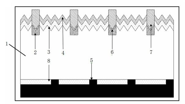
[0048] Such as figure 1 A kind of N-type monocrystalline silicon substrate PN junction inversion layer battery shown, it comprises: N-type monocrystalline silicon substrate 1, front electrode, back electrode, front surface Al2O3 thin film film 3 and silicon nitride Thin film 4; front electrode includes: local boron diffusion region 2, Ti / Pb thin film 6 and front surface metal electrode 7; back electrode includes: back surface metal electrode 5 and back surface aluminum oxide film 8.
[0049] The front surface of the N-type single crystal silicon substrate 1 is attached with the front surface aluminum oxide film 3, and the front surface of the front surface aluminum oxide film 3 is attached with a silicon nitride film 4; There is a groove, and the front electrode is arranged in the groove, and the front electrode is arranged sequentially from the inside to the outside: local boron diffusion region 2, Ti / Pb thin film 6 and front surface metal electrode 7; N-type single crystal s...
Embodiment 2
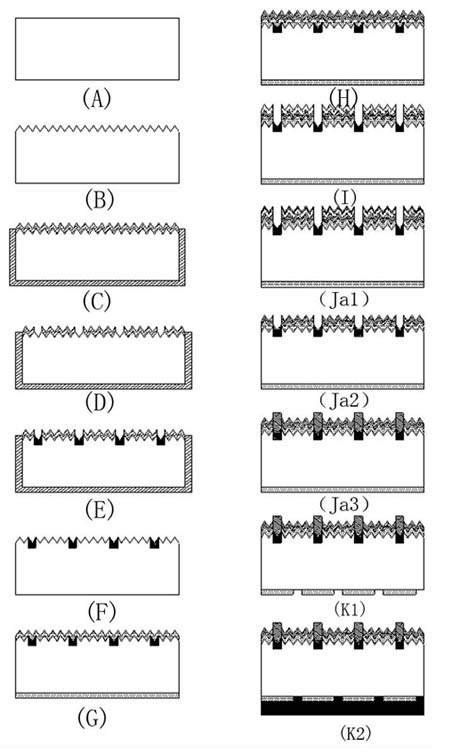
[0069] In this embodiment, the N-type monocrystalline silicon substrate PN junction inversion layer battery is the same as in Embodiment 1, and the manufacturing method of the N-type monocrystalline silicon substrate PN junction inversion layer battery is as follows image 3 As shown, the specific steps are as follows:
[0070] (A) Prepare an N-type single crystal silicon substrate with a resistivity of 6??cm;
[0071] (B) Use potassium hydroxide solution to texture the surface of the N-type single crystal silicon substrate, prepare a pyramid-shaped flame structure on the surface of the N-type single crystal silicon substrate, and use a mixed solution of hydrochloric acid and hydrofluoric acid to carry out Chemical cleaning; the concentration range of potassium hydroxide solution is 2.5%; in the mixed solution of hydrochloric acid and hydrofluoric acid, the ratio of hydrochloric acid: hydrofluoric acid is 1:2.5; the concentration of the mixed solution of hydrochloric acid a...
Embodiment 3
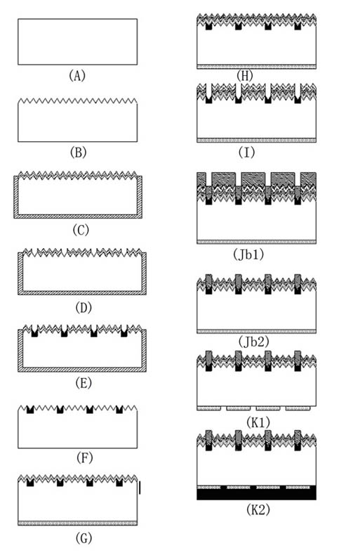
[0087] In this embodiment, the N-type monocrystalline silicon substrate PN junction inversion layer battery is the same as in Embodiment 1, and the manufacturing method of the N-type monocrystalline silicon substrate PN junction inversion layer battery is as follows image 3 As shown, the specific steps are as follows:
[0088] (A) Prepare an N-type single crystal silicon substrate with a resistivity of 5.5 cm;
[0089] (B) Use sodium hydroxide solution to texture the surface of the N-type single crystal silicon substrate, prepare a pyramid-shaped flame structure on the surface of the N-type single crystal silicon substrate, and use a mixed solution of hydrochloric acid and hydrofluoric acid to carry out Chemical cleaning; the concentration range of sodium hydroxide solution is 1%; in the mixed solution of hydrochloric acid and hydrofluoric acid, the ratio of hydrochloric acid: hydrofluoric acid is 1:3; the concentration of the mixed solution of hydrochloric acid and hydrof...
PUM
| Property | Measurement | Unit |
|---|---|---|
| Thickness | aaaaa | aaaaa |
| Thickness | aaaaa | aaaaa |
| Width | aaaaa | aaaaa |
Abstract
Description
Claims
Application Information
 - R&D Engineer
- R&D Manager
- IP Professional
- Industry Leading Data Capabilities
- Powerful AI technology
- Patent DNA Extraction
Browse by: Latest US Patents, China's latest patents, Technical Efficacy Thesaurus, Application Domain, Technology Topic, Popular Technical Reports.
© 2024 PatSnap. All rights reserved.Legal|Privacy policy|Modern Slavery Act Transparency Statement|Sitemap|About US| Contact US: help@patsnap.com


