Magnetic random access memory, magnetic logic device and spinning microwave oscillator
A random access memory and magnetic technology, applied in the field of magnetic logic devices and spin microwave oscillators, magnetic random access memory, and spin microwave oscillators, can solve the problem of limiting application range, device structure damage, and affecting device service life And other issues
- Summary
- Abstract
- Description
- Claims
- Application Information
AI Technical Summary
Problems solved by technology
Method used
Image
Examples
Embodiment 1
[0089] Figure 2B It is a cross-sectional view of a magnetic random access memory cell (MRAM cell) using the above-mentioned magnetic multilayer film memory cell with the Rashba effect according to Embodiment 1 of the present invention. It can be seen from the figure that the entire MRAM cell includes layers 1a, 1b, 1c, 1d, 1e, 1f, 1g, and the non-functional regions in these layers are made of insulating buried dielectric such as SiO 2 etc. buried, wherein the metal wiring layer has three layers, that is, the layer 1d where the read bit line BL1 4c is located, the layer 1f where the write bit line BL2 4d is located, and the layer 1b where the ground line GND 4a and the transition metal layer TM 4b are located. Wherein, the two bit lines BL1 4c and BL24d are respectively arranged above the magnetic multilayer film memory unit ML 6 , are separated from each other by an insulating layer 1e, and are perpendicular to the word line 2 . The magnetic multilayer film memory cell ML6 i...
Embodiment 2
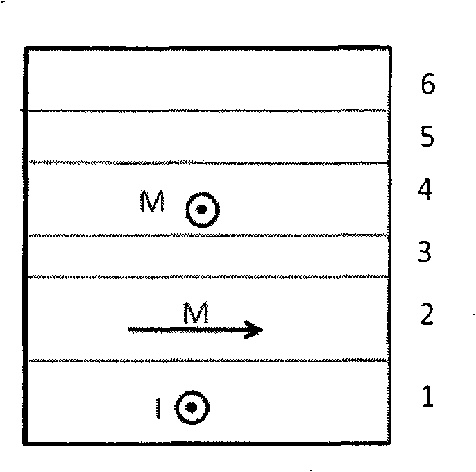
[0095] The MRAM unit was manufactured in the same manner as in Example 1, except for the magnetic multilayer memory unit. The magnetic multilayer film storage unit is: in Si / SiO 2 On the substrate, the non-magnetic layer Pt (1-5nm) and the ferromagnetic layer LaSrMnO are grown sequentially. x (3~5nm), then grow the intermediate layer CaMnO (1~2nm), the pinned ferromagnetic layer CoFe (2~5nm), the antiferromagnetic pinning layer IrMn (10nm), and the covering layer Ta (5nm); the magnetic The cross section of the multilayer film memory unit is a rectangular ring, the inner ring width of the rectangular ring is 50000nm, the ring width is 1000nm, and the ratio of the inner ring width to the length is 1:5.
Embodiment 3
[0097] The MRAM unit was manufactured in the same manner as in Example 1, except for the magnetic multilayer memory unit. The magnetic multilayer film storage unit is: firstly, in Si / SiO 2 On the substrate, the non-magnetic layer Pt (1-5nm) and the ferromagnetic layer GaMnAs (3-5nm) are grown sequentially, and then the intermediate layer CaAs (1-2nm) is grown, and the ferromagnetic layer CoFe (2-5nm) is pinned. The ferromagnetic pinning layer IrMn (10nm), the covering layer Ta (5nm), the cross section of the magnetic multilayer film storage unit is circular, and its diameter is 10000nm.
PUM
| Property | Measurement | Unit |
|---|---|---|
| thickness | aaaaa | aaaaa |
| thickness | aaaaa | aaaaa |
| width | aaaaa | aaaaa |
Abstract
Description
Claims
Application Information
 - R&D
- Intellectual Property
- Life Sciences
- Materials
- Tech Scout
- Unparalleled Data Quality
- Higher Quality Content
- 60% Fewer Hallucinations
Browse by: Latest US Patents, China's latest patents, Technical Efficacy Thesaurus, Application Domain, Technology Topic, Popular Technical Reports.
© 2025 PatSnap. All rights reserved.Legal|Privacy policy|Modern Slavery Act Transparency Statement|Sitemap|About US| Contact US: help@patsnap.com


