Storage element and storage device

A technology for storage elements and storage devices, which is applied in the direction of electrical components, information storage, static memory, etc., can solve problems such as inability to maintain information and changes in resistance value, and achieve excellent resistance value retention characteristics, improved resistance value retention characteristics, and improved Effect of resistance value retention characteristics

Active Publication Date: 2010-06-30
SONY CORP
View PDF0 Cites 16 Cited by
  • Summary
  • Abstract
  • Description
  • Claims
  • Application Information

AI Technical Summary

Problems solved by technology

[0008] However, each of the memory elements having the above-mentioned configuration has the following problem: when the memory element is left for a long time or placed in a temperature environment higher than room temperature, the memory state in which the resistance value of the ionic conductor is low (for example, In "1") or in an erased state (such as "0") in which the resistance value of the ionic conductor is high, the resistance value changes and information cannot be retained

Method used


Image

  • Storage element and storage device
  • Storage element and storage device
  • Storage element and storage device

Examples


example 1

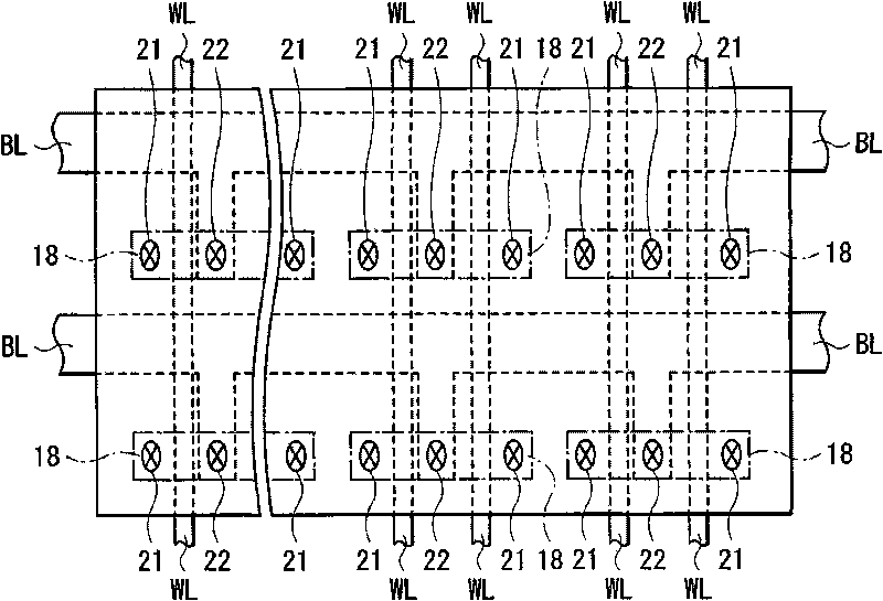
[0072] Such as figure 2 and image 3 As shown, first, a MOS transistor is formed on a semiconductor substrate 11 . Then, an insulating layer is formed to cover the surface of the semiconductor substrate 11, and via holes are formed on the insulating layer. Next, an electrode material composed of W (tungsten) is filled inside the through hole by CVD (Chemical Vapor Deposition), and its surface is planarized by CMP (Chemical Mechanical Polishing). Furthermore, these processes are repeated to form plug layer 15 , metal wiring layer 16 , plug layer 17 , and lower electrode 1 . Furthermore, the lower electrode 1 is patterned for each memory cell. The size of the opening of the lower electrode 1 is arranged to have a diameter of 300 nm. Next, etching of about 1 nm was performed by reverse sputtering using a radio frequency power source to remove oxides on the upper surface of lower electrode 1 . At this time, the surface of the lower electrode 1 is planarized so that the heigh...

example 2-5

[0081] In Example 2-5, in the ion source layer 3, other transition metal elements Ta, Cr, Ti, and W were used as metal elements to be ionized. The film thicknesses were all 45 nm.

example 2

[0082] Example 2: Ta20%-Te40%-Al40% (atomic %)


PUM

PropertyMeasurementUnit
thicknessaaaaaaaaaa

Abstract

The invention provides a resistance variation type storage device improved in ability to hold resistance values in writing and erasure states. A storage layer 5 comprising a high resistance layer 2 and an ionization layer 3 is provided between a lower electrode 1 and an upper electrode 4. The ionization layer 3 contains Zr (zirconium) and Al (aluminum) as metal elements to be cationized as well as an ion conductive material (anion element) such as S (sulfur), Se (selenium), and Te (tellurium) (chalcogenide element). An equivalent ratio represented by equivalent ratio=(valence of cations*number of moles) / (valence of anions*number of moles) is 0.5 to 1.5, and consequently holding characteristics of writing and erasure states are improved.

Description

technical field [0001] The present invention relates to a memory element and a memory device capable of storing two or more pieces of information by changing the electrical characteristics of a memory layer including an ion source layer. Background technique [0002] DRAM (Dynamic Random Access Memory), which is fast in operation and high in density, has been widely used as RAM (Random Access Memory) in information devices such as computers. However, DRAM has a complicated manufacturing process and high production cost compared with general logic circuit LSI (Large Scale Integration) or signal processing used in electronic equipment. Also, DRAM is a volatile memory that loses information when its power is cut off. Therefore, it is necessary to frequently perform refresh operations, that is, perform operations of reading out written information (data), performing reamplification, and performing rewriting again. [0003] Therefore, as a nonvolatile memory whose stored inform...

Claims


Application Information

Patent Timeline
Patent Type & Authority Applications(China)
IPC IPC(8): H01L27/10H01L45/00H01L49/00
CPCH01L27/2436G11C11/5614H01L27/101H01L45/085H01L45/1266H01L45/1625H01L45/143H01L45/141H01L45/145H01L27/2472H01L45/144G11C13/0011H01L45/142H01L45/1233H10B63/82H10B63/30H10N70/245H10N70/8416H10N70/826H10N70/8833
Inventor 大场和博水口徹也保田周一郎
Owner SONY CORP
Why Eureka
Try Eureka