Semiconductor device and method of fabricating the same

A manufacturing method, semiconductor technology, applied in semiconductor/solid-state device manufacturing, semiconductor devices, electrical components, etc., can solve problems such as increase and deterioration of retention characteristics, and achieve the effect of preventing movable ions from moving

Inactive Publication Date: 2009-01-21
DONGBU HITEK CO LTD
View PDF1 Cites 4 Cited by
  • Summary
  • Abstract
  • Description
  • Claims
  • Application Information

AI Technical Summary

Problems solved by technology

In the TEOS region, the distance between the barrier ribs (barrierrib) increases due to the stretching force, and mobile ions that cause charge loss and charge gain easily move into the increased space between the barrier ribs, so that the characteristic ( retention characteristics) deterioration

Method used


Image

  • Semiconductor device and method of fabricating the same
  • Semiconductor device and method of fabricating the same
  • Semiconductor device and method of fabricating the same

Examples


manufacture example

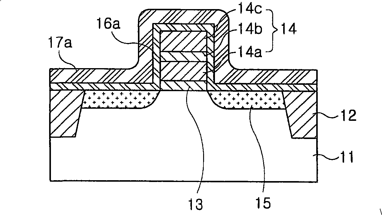
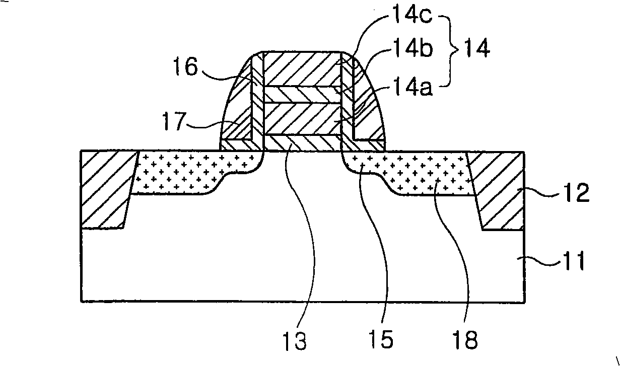
[0020] A method of manufacturing a semiconductor device such as a flash memory device is provided, wherein a blocking nitride layer is given compressive stress using an ion implantation process to prevent movement of mobile ions. Thus, the effects of charge loss and charge gain in the flash memory device are minimized.

[0021] Such as Figure 2A As shown in the example in FIG. 1 , gate insulating layer 103 and gate electrode 104 are formed on and / or over the active region of semiconductor substrate 101 defined by isolation layer 102 . A lightly doped (LDD) region 105 having a shallow trench isolation (STI) structure may be formed in an active region of the semiconductor substrate 101 .

[0022] In order to form the isolation layer 102, a pad insulating layer having a predetermined thickness may be formed on and / or over the semiconductor substrate 101, and then the pad insulating layer is etched by a photolithography process and an etching process using an isolation mask to f...


PUM


Abstract

A method of fabricating a semiconductor device includes forming first spacers formed of a TEOS layer and second spacers formed of a first nitride layer on sidewalls of a gate electrode formed on a semiconductor substrate, and then forming source / drain regions in the semiconductor substrate using the first and second spacers and the gate electrode as masks, and then removing the second spacers, and then depositing a second nitride layer on an entire surface of the semiconductor substrate, and then implanting ions into the second nitride layer to generate compressive stress, and then etching the second nitride layer to form barrier nitride layers on the side walls of the first spacers. Because the barrier nitride has compressive stress, it is possible to prevent the movement of mobile ions, minimize influence on charge loss and charge gain in a flash memory device, and enhance a retention characteristic.

Description

[0001] This application claims priority from Korean Patent Application No. 10-2007-0071613 (filed Jul. 18, 2007), the entire contents of which are hereby incorporated by reference. technical field [0002] The present invention relates to a semiconductor device and a manufacturing method thereof capable of restricting movement of mobile ions to minimize charge loss and charge gain and improve retention characteristics. Background technique [0003] Such as Figure 1A As shown, the manufacturing process of a semiconductor device such as a NOR flash memory may include the following steps: forming an isolation layer 12 with a shallow trench isolation (STI) structure in a semiconductor substrate 11; Gate insulating layer 13 and gate electrode 14 composed of first polysilicon layer 14a, insulating layer 14b and second polysilicon layer 14c. A lightly doped drain (LDD) region 15 may then be formed using the gate electrode 14 as a mask. [0004] Such as Figure 1B As shown in the...

Claims


Application Information

Patent Timeline
Patent Type & Authority Applications(China)
IPC IPC(8): H01L21/336H01L29/78
CPCH01L29/7881H01L21/26586H01L29/7843H01L29/66825H01L21/28273H01L29/6656H01L29/40114H01L21/265H01L21/28141
Inventor 朴真何
Owner DONGBU HITEK CO LTD
Why Eureka
Try Eureka