


Quick Research
Generate reliable direction feasibility study reports for your R&D in just a few steps.

Technical Q&A
Discover and master advanced knowledge NOW. Basics, ideas, possibilities, all at once.

Find Solutions
As an expert in R&D theories, this can generate solutions to your technical problems instantly.

Evaluate Feasibility
Analyze your overall solution with one click, know your potential R&D risks in advance.

Monitor Landscape
Get weekly tech updates, stay abreast of the latest tech innovations and key insights.
Circuit board and method for manufacturing the same
A technology of circuit substrate and manufacturing method, applied in printed circuit manufacturing, printed circuit, printed circuit and other directions, can solve problems such as difficulty in forming wiring, increase in processing steps, miniaturization of wiring, difficulty in high density, etc.
- Summary
- Abstract
- Description
- Claims
- Application Information
AI Technical Summary
Problems solved by technology
Method used
Image

Examples
Embodiment approach 1
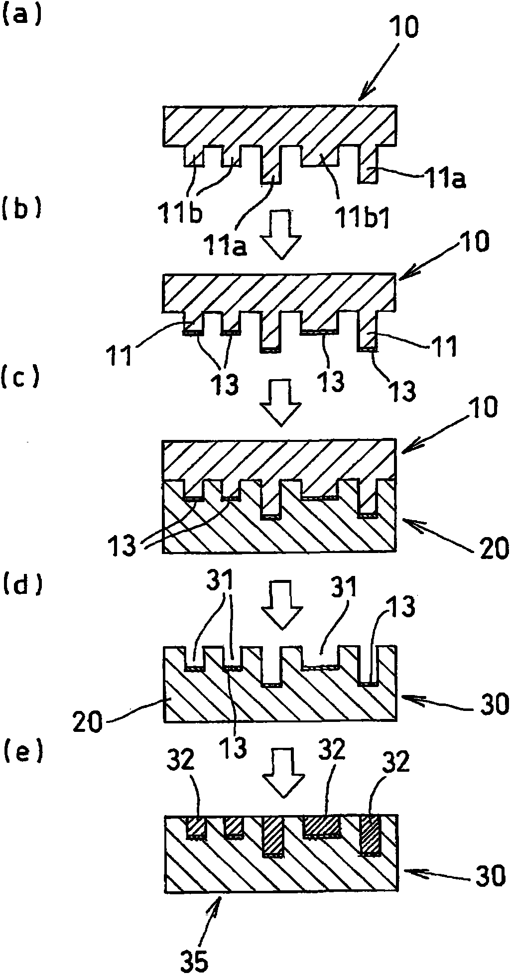
[0027] figure 1 The first embodiment of the method for manufacturing a circuit board of the present invention is shown in order of steps. exist figure 1 Among them, 10 is a casting mold, and a convex portion corresponding to a circuit pattern formed on the surface of the circuit board to be obtained is formed on the flat surface side of a nickel alloy plate having at least one flat surface by a conventionally known electroforming process. 11. like figure 1 As shown in a, two types of convex portions 11 a and convex portions 11 b having different heights are formed on the mold 10 . The convex part 11b1 which is one of the convex parts 11b is wider than the other convex part.
[0028] The width of the protrusions 11a and 11b is 5 μm, the width of the protrusion 11b1 is 20 μm, the distance between the protrusions is 5 μm, the height of the protrusion 11a is 15 μm, and the height of the protrusion 11b is 5 μm.
[0029] Next, if figure 1 As shown in b, on the front end of the...
Embodiment approach 2
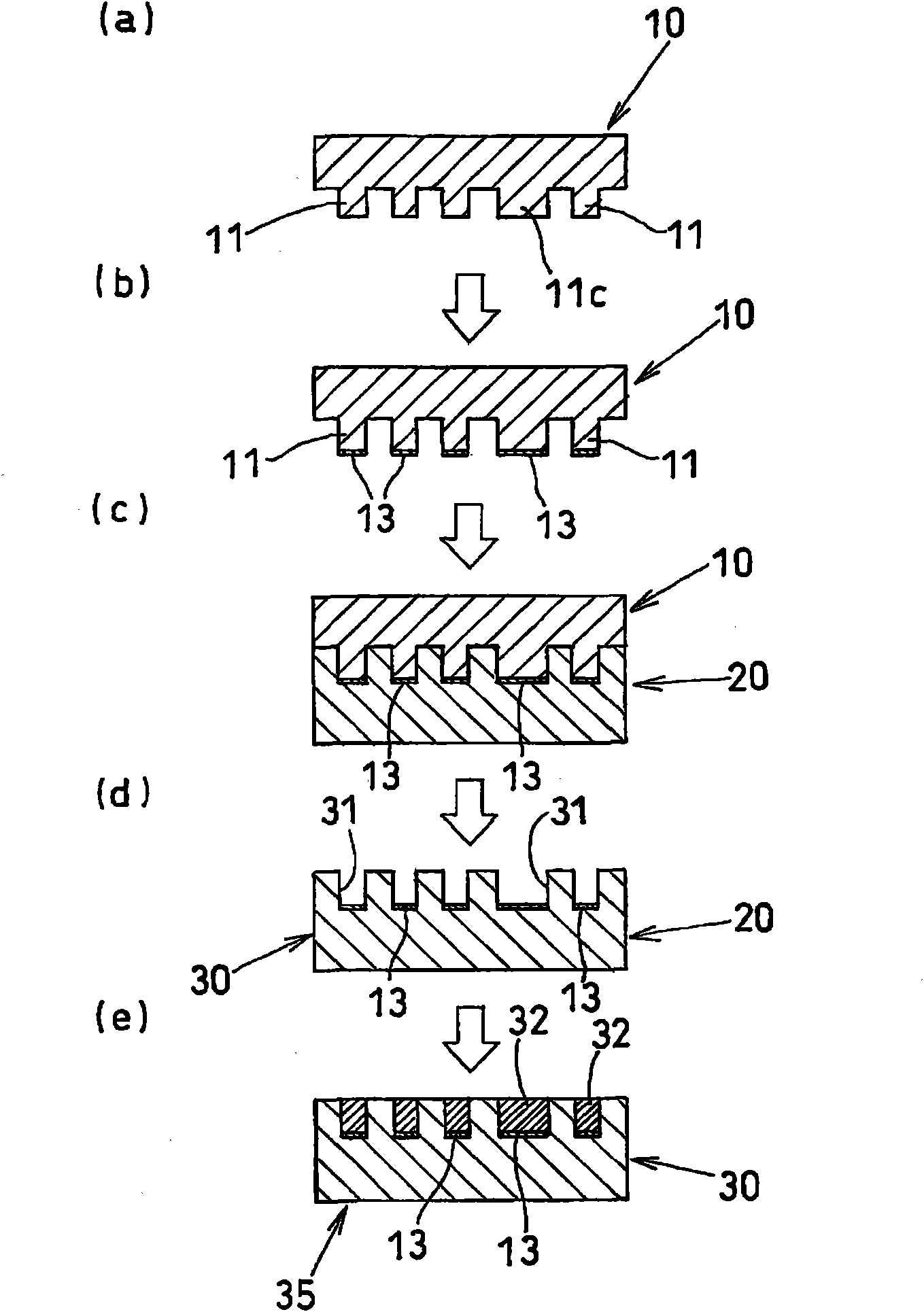
[0035] figure 2 The second embodiment of the method for manufacturing a circuit board of the present invention is shown in order of steps. Here, as the material of the casting mold 10, a glass plate with a flat surface is used, and by performing a conventionally known sandblasting treatment, such as figure 2 As shown in a, the convex portion 11 is formed on the flat surface side of the glass plate. The protrusions 11 have a width of 5 μm and a height of 10 μm, and one protrusion 11 c has a width of 10 μm. In addition, the distance between the protrusions was 5 μm.
[0036] Next, a silver paste mainly composed of silver nanoparticles with an average particle diameter of 20 nm is stretch-coated on the PET plate with a thickness of 2 μm by using a bar coater or the like, and the convex portion 11 side of the mold 10 is pressed against it. ,like figure 2 As shown in b, the casting mold 10 in which the silver paste 13 was applied to the tip of the convex portion 11 was obtai...
Embodiment approach 3
[0041] Although not shown, as the material of the mold 10 , a quartz plate with one surface flat was used, and similar to Embodiment 2, convex portions with a width of 50 μm and a height of 50 μm were formed. The distance between the protrusions was 10 μm.
[0042] Next, the silver paste mainly composed of silver nano-ions with an average particle diameter of 5 nm is coated with a thickness of 5 μm by using a bar coater or the like on the PET plate, and the convex portion 11 side of the mold 10 is pressed against it. Thus, the mold 10 in which the silver paste was applied to the tip of the convex portion 11 was obtained.
[0043] A polycarbonate resin film having a thickness of 80 μm was placed on a glass plate, the convex portion 11 side of the mold 10 was pressed thereon, and heat treatment was performed at 170° C. for 10 minutes under vacuum.
[0044] When the mold 10 is removed after normal temperature and pressure, the resin molded article 30 in which the shape of the co...
PUM
 Abstract
Description
Claims
Application Information
 - R&D Engineer
- R&D Manager
- IP Professional
- Industry Leading Data Capabilities
- Powerful AI technology
- Patent DNA Extraction
Browse by: Latest US Patents, China's latest patents, Technical Efficacy Thesaurus, Application Domain, Technology Topic, Popular Technical Reports.
© 2024 PatSnap. All rights reserved.Legal|Privacy policy|Modern Slavery Act Transparency Statement|Sitemap|About US| Contact US: help@patsnap.com