
Silver copper composite oxide film material for photoelectric semiconductor

A composite oxide and optoelectronic semiconductor technology, which is applied in the direction of silver compounds, silver compounds, semiconductor devices, etc., can solve the problems of inability to absorb solar photons, low light absorption coefficient, low energy utilization rate, etc., and achieve good comprehensive performance and excellent preparation process Simplicity, the effect of reducing the use of scarce elements

Inactive Publication Date: 2009-03-11
KUNMING UNIV OF SCI & TECH
View PDF0 Cites 7 Cited by
  • Summary
  • Abstract
  • Description
  • Claims
  • Application Information

AI Technical Summary

Problems solved by technology

The defects of currently known photoelectric materials are summarized as follows: polysilicon material is used in most solar materials because of its low price, but it is an indirect band gap semiconductor material, which cannot absorb solar photons very well, and its transition is limited to a certain extent , resulting in low light absorption coefficient and low energy utilization efficiency; compared with them, compound semiconductor optoelectronic materials have good photoelectric absorption coefficient, but some contain scarce elements, such as indium (In), selenium (Se), etc. The compound semiconductor materials contain toxic elements, such as cadmium (Gd), arsenic (As), etc., and the overall process of compound semiconductor materials is more complicated, resulting in higher costs, and it is still difficult to compete with polysilicon materials.

Method used


Image

  • Silver copper composite oxide film material for photoelectric semiconductor
  • Silver copper composite oxide film material for photoelectric semiconductor
  • Silver copper composite oxide film material for photoelectric semiconductor

Examples


Embodiment 1

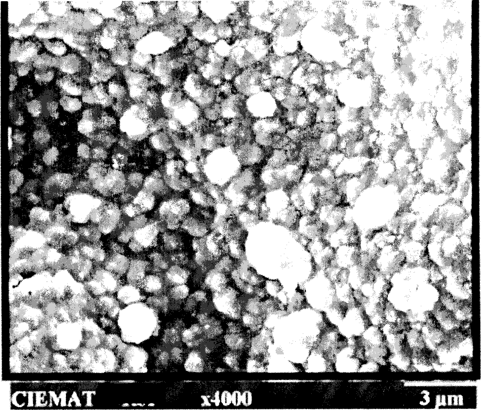
[0045] Press 38% copper powder (percentage by weight), 62% silver powder (percentage by weight), after mixing for 4 hours, bidirectionally press in a steel mold to form a biscuit, and the molding pressure of the biscuit is 650MPa; The ingot was sintered in an oxygen-containing atmosphere for 3 hours; the ingot was sputtered and deposited on a glass substrate for about 30 minutes, and further oxidized to obtain a silver-copper composite oxide (AgCuO 2 and a small amount of AgCuO 3 )film.

Embodiment 2

[0047] Prepare raw materials according to the ratio of 39% copper powder (weight percentage), 60.2% silver powder (weight percentage), cobalt powder (Co) 0.8% (weight percentage), after mixing for 6 hours, two-way pressing in the steel mold becomes plain Blank, the forming pressure of the blank is 450MPa; the blank is further pressed by 300MPa cold isostatic pressing, and the blank is sintered at 700°C for 4 hours in an oxygen-containing atmosphere to form an ingot, and the ingot is deposited on a glass substrate by sputtering, and the time is about 50 minutes, and through further oxidation treatment, obtain the cobalt-doped silver-copper composite oxide (AgCuO 2 and a small amount of AgCuO 3 )film.

Embodiment 3

[0049] According to 98.6% of the silver-copper alloy powder (wherein the weight percent content of copper is 37% of the silver-copper alloy powder), 0.7% Zn (zinc), 0.5% Mn (manganese) and 0.4% In (indium) of the alloy powder weight are added Add elements, prepare raw materials in proportion, after 8 hours of mixing, cold isostatic pressing is formed into a green body, the green body forming pressure is 250MPa; Sputtering deposition on the bottom, the time is about 60 minutes, and after further oxidation treatment, a zinc-manganese-indium-doped silver-copper composite oxide (AgCuO 2 and a small amount of AgCuO 3 )film.


PUM

PropertyMeasurementUnit
band gapaaaaaaaaaa
band gapaaaaaaaaaa
particle sizeaaaaaaaaaa

Abstract

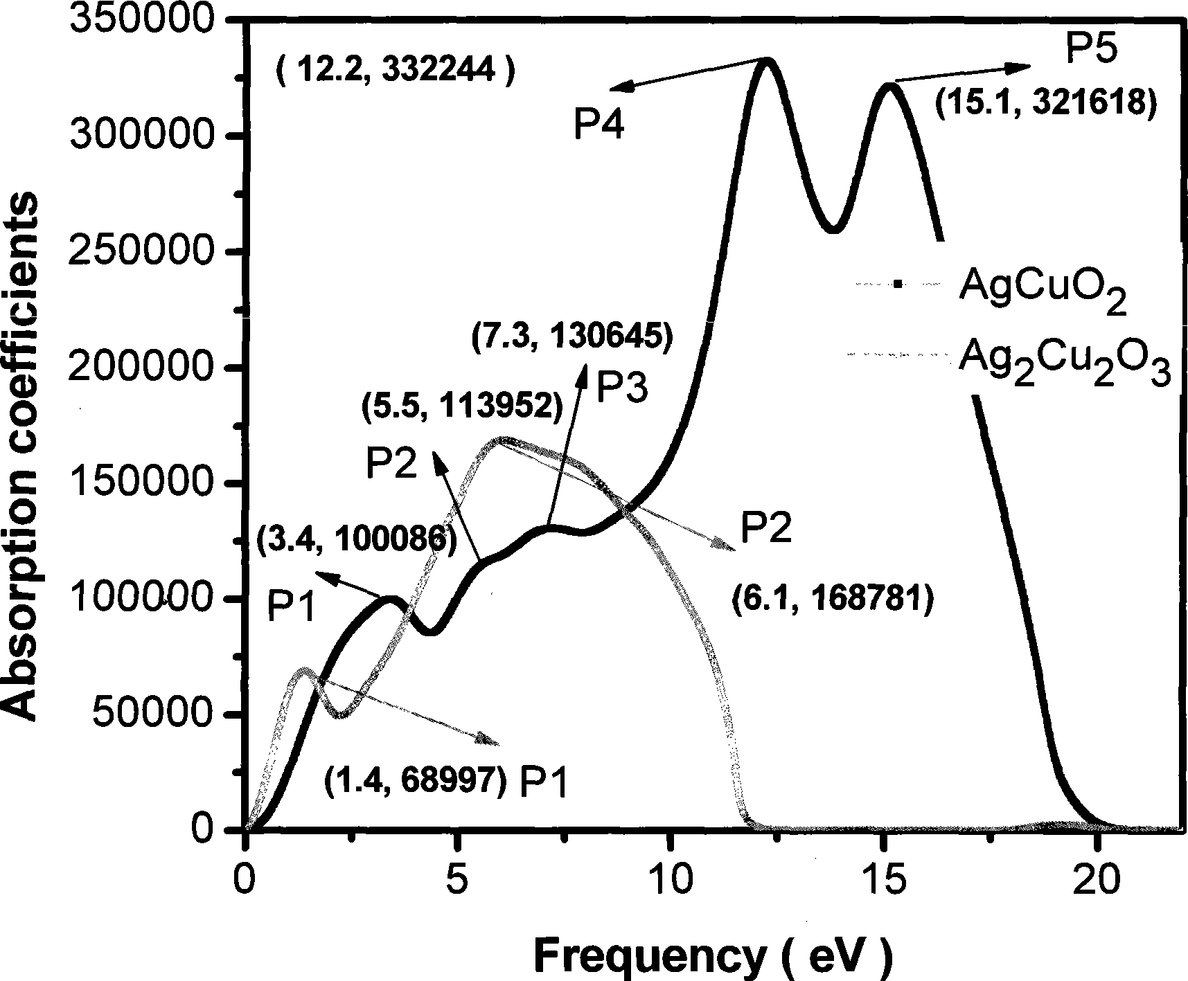
The invention discloses a novel photoelectric material which belongs to the photoelectric field and the semiconductor field. The photoelectric material takes silver powder, copper powder or silver copper alloy powder as the raw material, and a small amount of other elements as the forbidden bandwidth performance adjusting elements such as Al, P, S, V, Mn, Co, Ni, Zn, Ga, Ge, As, Se, Nb, Mo, In, Sb, and the like are added, so that target materials are produced by molding and oxidizing, and a composite oxide thin film (AgCuO2 and Ag2Cu2O3) of silver, copper and oxygen is obtained by electric pulse deposition or magnetic-controlled sputtering deposition. The film can form the structure and the proportion of oxide through controlling partial pressure adjustment of oxygen, the photoabsorption coefficient and the reflectance ratio can be adjusted in a wider range, the structure is stable, the comprehensive performance is good, and the film can be practically applied to the field of the special photoelectric conversion material. The production cost of the novel photoelectric material is lower than that of the present chemical compound photoelectric conversion material, the performance is superior, the entire production process is simple and is easy to be controlled without pollution or less pollution, and the mass production can be performed; the relevant products can be widely applied to the solar energy materials, the space cell paddle materials, and the high-energy photon absorption.

Description

technical field [0001] The invention relates to a novel photoelectric material, in particular to a composite oxide thin film of a compound photoelectric semiconductor material and its preparation method and application. It belongs to the technical field of photoelectric conversion materials. Background technique: [0002] The known photoelectric conversion materials mainly include the following types: [0003] 1. Monocrystalline silicon optoelectronic semiconductor materials [0004] Monocrystalline silicon solar cell is a relatively advanced type of solar cell currently developed. Its structure and production process have been finalized, and its products have been widely used in space and on the ground. This kind of solar cell uses high-purity monocrystalline silicon rods as raw materials, and the purity requirement is more than 99.999%. It is characterized by high photoelectric conversion efficiency and higher light absorption coefficient than crystalline silicon, but i...

Claims


Application Information

Patent Timeline
Patent Type & Authority Applications(China)
IPC IPC(8): H01L31/032H01L31/18C01G3/02C01G5/00
CPCY02P70/50
Inventor 冯晶陈敬超肖冰于杰杜晔平周荣武淑珍
Owner KUNMING UNIV OF SCI & TECH
Learn More