Photomask detection method and on-line immediate photomask detection method

A detection method and photomask technology, applied in the field of photomask detection, can solve the problems of increased cost, low sampling rate, time spent, etc.

Active Publication Date: 2009-01-14
UNITED MICROELECTRONICS CORP
View PDF0 Cites 5 Cited by
  • Summary
  • Abstract
  • Description
  • Claims
  • Application Information

AI Technical Summary

Problems solved by technology

As a result, it takes a long time to wait for the detection results, and the sampling rate of the detection is low
Furthermore, the above-mentioned photomask inspection machine is usually expensive, resulting in a substantial increase in cost

Method used


Image

  • Photomask detection method and on-line immediate photomask detection method
  • Photomask detection method and on-line immediate photomask detection method
  • Photomask detection method and on-line immediate photomask detection method

Examples


Embodiment Construction

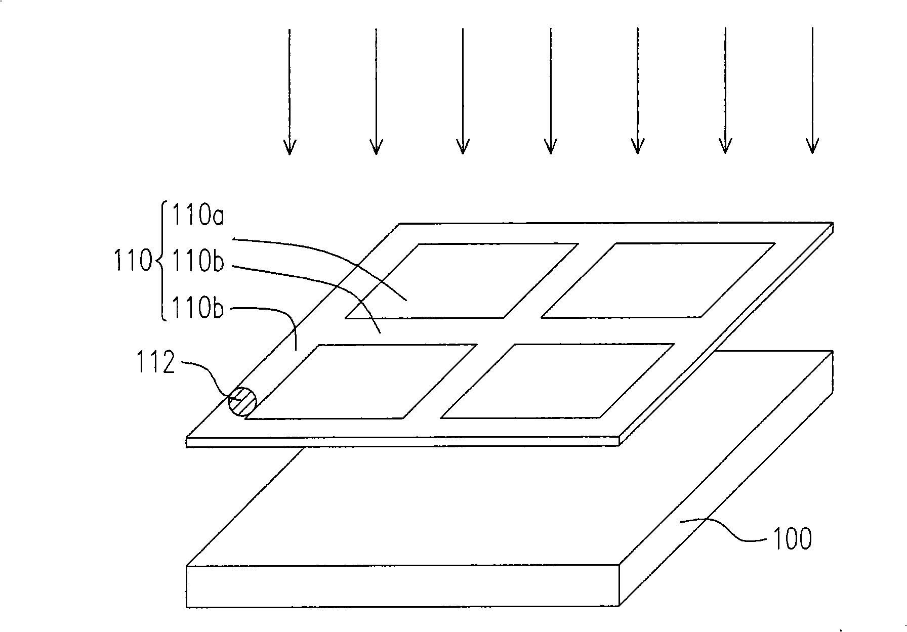
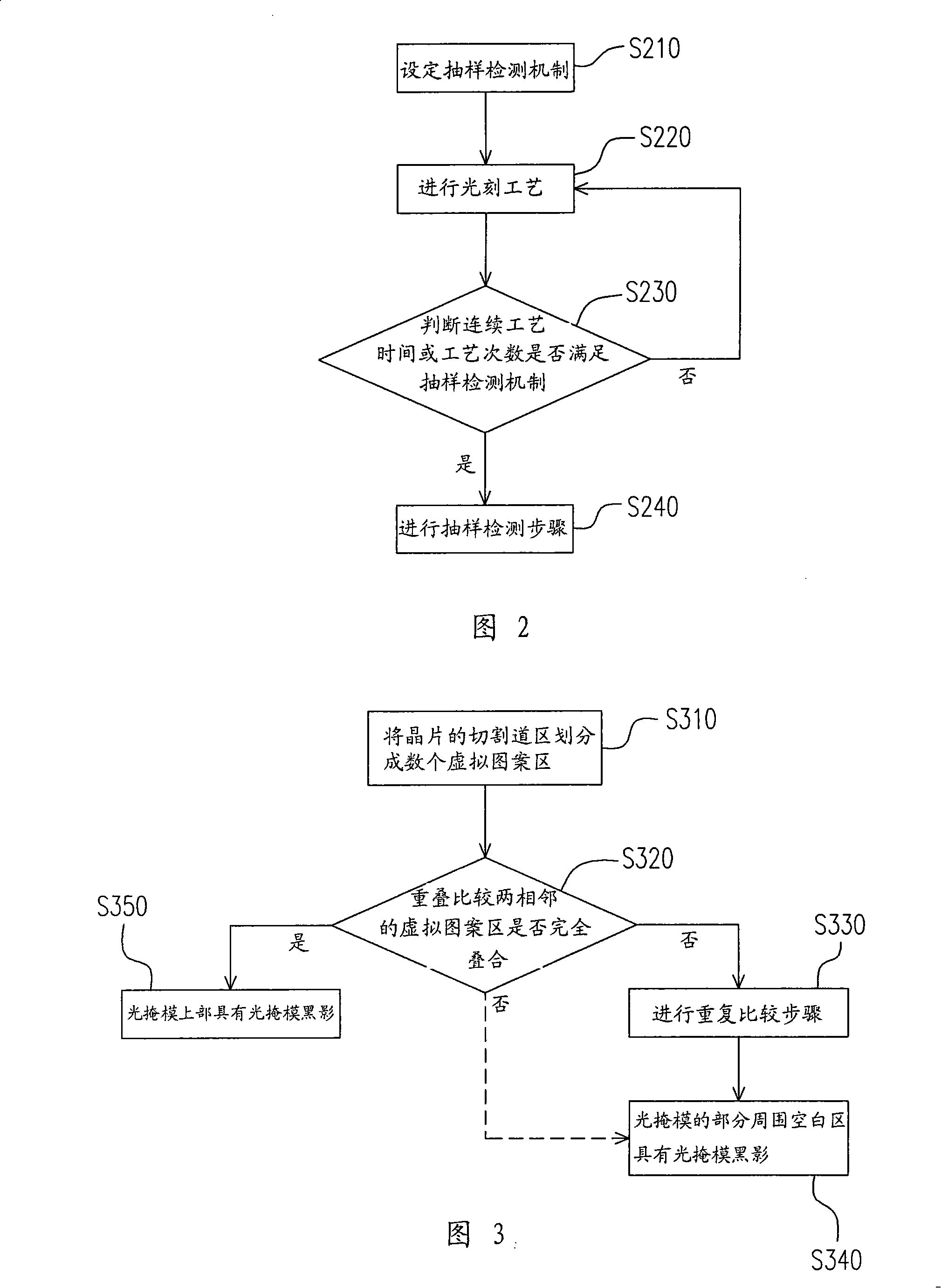
[0041] In the photolithography process, the exposure process will cause photomask shadows on the photomask, and the photomask shadows will gradually expand with the increase of process time, which will not only affect the subsequent process, but also affect the reliability of the process And the cost of many processes. Therefore, when performing the photolithography process, the present invention also considers the influence of the shadow of the photomask on the pattern transfer, compares the wafers that have completed the process steps, and effectively detects whether the shadow of the photomask is formed on the photomask. The implementation of the online real-time photomask inspection method of the present invention will be described below in the form of a flow chart.

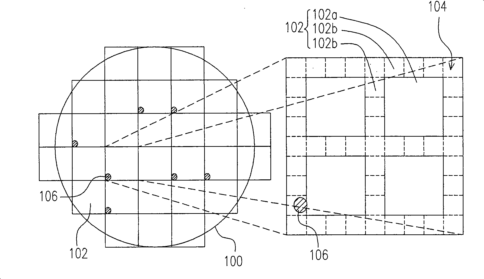
[0042] Figure 1A It is a schematic diagram of a photolithography process according to an embodiment of the present invention. Figure 1B It is a schematic top view of a wafer according to an embodiment of t...


PUM


Abstract

The invention discloses a photomask detecting method which is applicable to the photomasks provided with a pattern zone and a blank zone. Firstly, a chip for carrying out lithography in virtue of the photomask is provided. The chip is provided with a plurality of exposure zones and each exposure zone is provided with a component pattern zone, wherein, each component pattern zone is surrounded by a cutting channel zone and corresponds to the photomask pattern zone and the cutting channel zone corresponds to the photomask blank zone. Secondly, the cutting channel zone is divided into a plurality of virtual pattern zones. Then a step of two-two overlapping comparison is carried out for the virtual pattern zones, and when at least one of the virtual pattern zones dose not fully overlap with other virtual pattern zones, a photomask shadow appears on parts of the blank zone of the photomask corresponding to the virtual pattern zone without full overlapping.

Description

technical field [0001] The invention relates to a photomask detection method, and in particular to an online real-time photomask detection method. Background technique [0002] Recently, semiconductors tend to shrink the design and development of circuit elements, and one of the most important steps in the whole semiconductor process is photolithography. Anything related to the semiconductor device structure, such as the pattern of each layer of thin film, is determined by the photolithography process to determine the size of its critical dimension (CD). Therefore, the accuracy of transferring the pattern on the photomask to the wafer (wafer) plays a very important role. If the pattern on the photomask is incorrect, the transfer of the pattern will be even more incorrect, thereby affecting the tolerance of critical dimensions on the wafer and reducing the resolution of exposure. [0003] When making a photomask, sulfuric acid is usually used to clean the photomask, so that...

Claims


Application Information

Patent Timeline
Patent Type & Authority Applications(China)
IPC IPC(8): G03F1/00G03F1/30
Inventor 杨忠彦张明哲
Owner UNITED MICROELECTRONICS CORP
Why Eureka
Try Eureka