Compound film hetero-junction having magnetoelectric effect and preparing method thereof
A composite film, magnetoelectric effect technology, applied in the fields of dielectric physics and magnetic physics, can solve the problems of weak magnetoelectric effect of composite film, limited stress transfer process, weak magnetostrictive performance, etc., to avoid stress constraints. , the effect of effective interface stress transfer and effective magnetoelectric coupling
- Summary
- Abstract
- Description
- Claims
- Application Information
AI Technical Summary
Problems solved by technology
Method used
Image
Examples
Embodiment 1
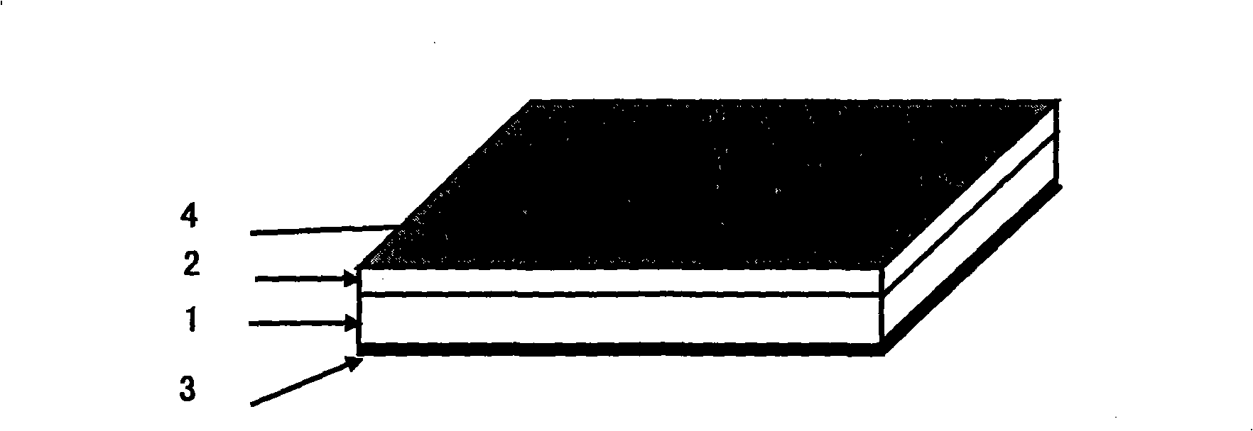
[0068] Example 1: SmFe 2 / PVDF nanocomposite film heterojunction. refer to figure 1 , SmFe 2 / PVDF nanocomposite film heterojunction consists of a polarized PVDF piezoelectric film layer 1 and SmFe with negative magnetostrictive effect 2 The nano film layer 2 is composed of a flat aluminum (Al) electrode 3 for output voltage on the lower surface of the PVDF piezoelectric film layer 1, and the SmFe 2 The upper surface of the nano film layer 2 has a flat platinum (Pt) electrode 4 for output voltage. Among them, the thickness of PVDF piezoelectric film is 20μm, SmFe 2 The thickness of the nano film layer is 200nm.
[0069] Preparation of the above SmFe 2 / PVDF nanocomposite film heterojunction method is as follows:
[0070] (1). Select SmFe 2 Alloy sheet as sputtering target;
[0071] (2). Coating an aluminum electrode on the bottom surface of the piezoelectric film of PVDF through polarization treatment;
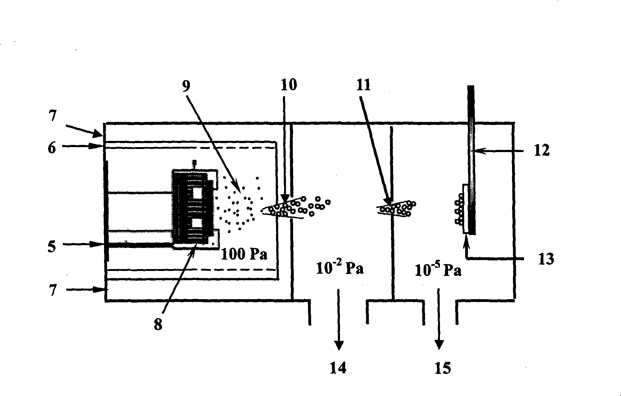
[0072] (3). Make the vacuum degree of the sample deposition cham...
Embodiment 2
[0078] Example 2: TbFe 2 / PVDF nanocomposite film heterojunction
[0079] The TbFe of this embodiment 2 The structure of the / PVDF nano-film heterojunction is similar to that of the nanocomposite film heterojunction in Example 1, consisting of a PVDF piezoelectric film layer with a thickness of 20 μm and a TbFe film with a magnetostrictive effect. 2 Nano film layer structure, wherein, the lower surface of the PVDF piezoelectric film layer has a planar Al electrode for output voltage, and the TbFe 2 The upper surface of the nano film layer has a layer of planar Pt electrodes for output voltage. The basic difference between the nanocomposite film heterojunction in this embodiment and the nanocomposite film heterojunction in Example 1 is that the rare earth iron alloy material used in this example is TbFe with positive magnetostrictive effect 2 Material, TbFe 2 The thickness of the nano film layer is 390nm.
[0080] The TbFe of this embodiment 2 The preparation method of th...
Embodiment 3
[0085] Example 3: Tb 0.7 Dy 0.3 Fe 2 / PVDF nanocomposite film heterojunction (the Tb 0.7 Dy 0.3 Fe 2 It is a commercial rare earth ferroalloy magnetostrictive material, the trade name is: Terfenol-D).
[0086] Tb of this embodiment 0.7 Dy 0.3 Fe 2 The structure of the / PVDF nano-film heterojunction is similar to that of the nanocomposite film heterojunction in Example 1, consisting of a PVDF piezoelectric film layer with a thickness of 20 μm and a Tb with magnetostrictive effect after polarization treatment. 0.7 Dy 0.3 Fe 2 Nano-film layer structure, wherein, the lower surface of the PVDF piezoelectric film layer has a planar Al electrode for output voltage, and the Tb 0.7 Dy 0.3 Fe 2 The upper surface of the nano film layer has a layer of planar Pt electrodes for output voltage. The basic difference between the nanocomposite film heterojunction in this embodiment and the nanocomposite film heterojunction in Example 1 is that the rare earth iron alloy material use...
PUM
| Property | Measurement | Unit |
|---|---|---|
| Thickness | aaaaa | aaaaa |
| Thickness | aaaaa | aaaaa |
| Diameter | aaaaa | aaaaa |
Abstract
Description
Claims
Application Information
 - R&D
- Intellectual Property
- Life Sciences
- Materials
- Tech Scout
- Unparalleled Data Quality
- Higher Quality Content
- 60% Fewer Hallucinations
Browse by: Latest US Patents, China's latest patents, Technical Efficacy Thesaurus, Application Domain, Technology Topic, Popular Technical Reports.
© 2025 PatSnap. All rights reserved.Legal|Privacy policy|Modern Slavery Act Transparency Statement|Sitemap|About US| Contact US: help@patsnap.com


